|
|||||||||||||||||||||||||||||||||||||
|
|
|||||||||||||||||||||||||||||||||||||
       |
Regular Articles Vol. 18, No. 10, pp. 38–45, Oct. 2020. https://doi.org/10.53829/ntr202010ra1 Ultralow Latency Optical Logic Operations with an Ultrasmall Silicon Wire Ψ GateAbstractElectronic computation circuits are composed of logic gates. However, due to the exponential increase in wiring resistance of miniaturized electronic components, both the increase in latency and energy consumption is becoming a serious problem. To overcome the electronic bottleneck, we developed an ultrasmall silicon-wire multimode interferometer called a Ψ (psi) gate for low-loss and high-speed optical logic operation. With a single Ψ gate, we can carry out Boolean logic operations (OR, XOR, AND, XNOR, NOR, and NAND) in telecom wavelength (1535–1565 nm) with an ultralow latency of ~30 fs. Such gates are expected to be used in novel photonics-electronics convergence processors for ultralow latency pattern matching and vector operations for photonic neural network applications. Keywords: optical logic gates, linear optics, silicon photonics
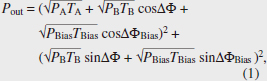
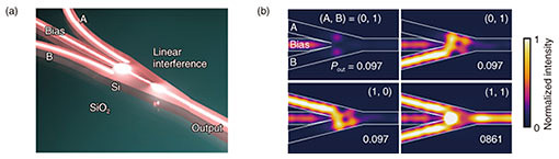
1. IntroductionData processing infrastructures based on complementary metal oxide semiconductors (CMOS) have seen continuous growth owing to the huge progress in semiconductor fabrication technologies. However, increases in leakage current and wiring resistance due to the miniaturization of electronic circuits will put an end to this continuous growth in the near future [1]. Accordingly, we are seeing accelerated exploration of novel technologies in all domains of science and technology towards the next generation of scalable data processing infrastructure. Moreover, latency has been worsening because the increase in wiring resistance also limits the response speed of electronic circuits (known as resister-capacitor time constant), which would limit the future development of applications related to communications security, real-time control, financial transactions, and so on. Note that latency can be reduced by inserting repeaters in electronic wires. This method is not energy efficient and would not help to overcome the traditional trade-off between latency and energy consumption. It is expected that this latency problem can be drastically mitigated using light for processing not only for communication because an optical signal can propagate through photonic circuits at the speed of light. Additionally, if the elemental photonic devices comprising a photonic circuit become smaller, the total optical pass length in the circuit will become shorter. Thus, further reducing device size lowers latency [2]. Our group developed high-performance micro/nanophotonic devices, e.g., nanolasers [3], nanophotodetectors [4], nanomodulators, and optical transistors [5], which should be fundamental building blocks for fabricating low-latency nanophotonic processors. We also developed the first high-performance ultralow-latency optical logic gate based on light-interference, called a Ψ (psi) gate based on its shape (Fig. 1(a)), as another building block [6]. In this article, we introduce the concept and a brief theoretical background of Ψ gates and the experimental demonstration of various optical logic operations with a single Ψ gate. We also present preliminary on-chip integration of a Ψ gate and other photonic components for stable operation. Next, we show how to use Ψ gates for optical multibit AND circuits and estimate latency, which is 10 times lower than the best case of CMOS electronic circuits. Finally, we conclude with the potential of using Ψ gates in ultralow-latency photo-electronic-converged accelerators. 2. Logic operations with a silicon wire Ψ gateLight-interference is a linear phenomenon, so it has been too primitive to carry out various logic operations, and the functions and performance were limited. However, almost all representative Boolean logic operations can be carried out with a single linear gate by introducing the concept of bias light and adjusting the input conditions [7]. Such multiple interference systems can be implemented using silica planer lightwave circuits [8], silicon (Si) photonics [9], and plasmonics [10]. The footprint of the gates is crucial for dense integration. Therefore, if we only need to make it as small as possible, we should choose plasmonics as the platform. However, we need to consider insertion loss to consider the configuration for multibit operations (discussed in Section 5). We found that the most promising platform is Si photonics. Our Ψ gate (Fig. 1(a)) has three input ports and one output port (the Ψ gate is a part of a 3 × 3 interferometer with two extra hidden radiation ports). Two of them are signal ports (A and B), and the center one is a bias port (denoted as Bias). The two sequences of the intensity modulated signals are input into A and B (relative input powers of both signals PA and PB are varied between P0 and P1) with a fixed relative phase relationship. In contrast, the intensity of the bias light is fixed at PBias. The optical output signal power Pout through a Ψ gate is then given as follows [6];
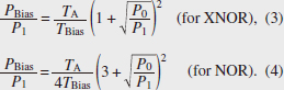
In this situation, we set TA = TB ~ 0.39, TBias ~ 0.20 (TA + TB + TBias ~ 0.98), ΔΦ = 0, ΔΦBias = π, and PBias ~ 0.48 for the maximum binary contrast (BC) of 9.54 dB [7]. From the simulated intensity distributions of Fig. 1(b), the operation result appears just after the multiple interference part of the Ψ gate. This means the AND operation is carried out by just passing the light through the 3-µm-long Ψ gate. Therefore, the physically limited computation latency of a single AND operation is ~30 fs. This latency is more than 100 times lower than that of CMOS electronics (~10 ps). From the Pout of (A, B) = (1, 1), we define signal loss (SL) as 10 log10 (Pout/P1) (SL becomes 0 dB when Pout = P1 = 1). By using the Si photonics platform, we can obtain SL < 0.5 dB. Even if we try to fabricate a similar interferometer based on loss-less half mirrors, SL becomes ~1.25 dB. As far as we know, there have been no reports on optical logic gates with such low SL. The required relative bias power PBias/P1 for the maximum BC for an AND operation can be derived from Eq. (1) as follows;
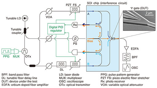
3. High-speed optical logic operationsA sample of a silicon wire Ψ gate was fabricated on a silicon-on-insulator (SOI) substrate with a 220-nm-thick top Si layer. An e-beam resist was spin-coated on the substrate, and the resist pattern was formed after e-beam writing and development. The resist pattern was transferred to the Si layer by using dry etching. After the resist was removed, polymer spot size converters [11] were fabricated for the input/output ports by using 2nd e-beam lithography. Figure 2 illustrates our setup for demonstrating high-speed logic operations. We used several off-chip optical components connected with several fiber patch cords. However, the relative phases of the input signals are always affected by phase fluctuations due to the mechanical vibrations of the fibers. To eliminate such fluctuation, we used fiber stretchers controlled using a digital proportional integral differential (PID) regulator. First, the laser light was split into two using a tunable coupler. One is intensity-modulated input for signal ports A and B, and the other is an invariant input for the bias port. To generate arbitral optical bit patterns, an optical transmitter connected to a pseudo random pulse pattern generator with a radio-frequency signal multiplexer was used (up to 64 Gbit/s). The generated optical bit patterns were separated into two by using a 3-dB coupler. After intensity tuning with a multi-channel variable optical attenuator, the bottom-side signal was delayed using a fiber delay line so that the Ψ gate under the test effectively had two different pseudo random bit patterns for signal ports A (top-side) and B (bottom-side). All the input and output lights were coupled to the SOI chip by using a lens module and lensed fiber. The output light was amplified through an erbium-doped fiber amplifier. After removing the amplified spontaneous emission noise by using an optical bandpass filter, the output bit patterns were observed using an optical sampling oscilloscope with a bandwidth of 70 GHz. For the optical phase lock loops between signals and bias light, we obtained an individual phase difference between signals and a bias light (the bias channel is set as the phase standard). The phase of the bias light was weakly modulated using the fiber-input phase shifter (PS) with 200 kHz for the dithering. The converted electrical signals through two channels of the photo receiver were input to a digital PID regulator. This PID regulator includes a high-voltage amplifier for directly driving the fiber stretcher.
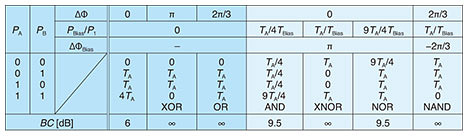
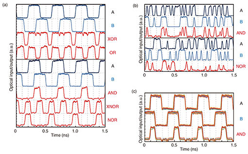
Figure 3 summarizes various logic operations obtained from a single Ψ gate. The output power of the tunable laser diode was set to 8 dBm for the demonstration. Figure 3(a) shows the input and output optical time waveforms of 10-Gbit/s XOR, OR, AND, XNOR, and NOR logic operations with proper input conditioning according to Table 1. We clearly demonstrated the basic concept of the linear optical logic operations. The XOR and OR operations do not require the bias input. In our demonstration, however, a fraction of PBias was required for optical phase locking. The AND, XNOR, and NOR operations exhibit BC of ~9.3 dB, > 10 dB, and ~9.0 dB with PBias/P1 ~ 0.62, 1.6, and 3.1, respectively. The experimental PBias/P1 fits well to the analytical prediction of Eqs. (2)–(4) by taking into account the finite extinction ratio (ER) of the input signals (ER = 10 log10(P1/P0) ~ 13–23 dB). Figure 3(b) shows the case for 40-Gbit/s pseudo random bit sequence AND and NOR operations. Both operations seemed to work with some degradation because of the finite rise/fall time of the input signals (~30 ps). However, the Ψ gate never became the bottleneck of the operation bandwidth because of the quite flat spectral response over 100 nm in the wavelength [6]. Figure 3(c) illustrates a 10-Gbit/s wavelength insensitive AND operation in telecom wavelength (1535–1565 nm). By calibrating PBias/P1 for each λ, a similar BC was achieved for all the tested input wavelengths. In this demonstration, the input signal bit sequences and operations were the same for all λ. It should be noted, however, that we can simultaneously carry out different operations for each wavelength channel by varying the input conditions (that is, totally independent parallel logic operations are possible up to the number of input channels with a single Ψ gate). This is unique and benefits our linear gates compared to nonlinear gates. Note that the demonstrated input wavelength range was actually limited by our setup, and the flatness of the transmission spectra and optical damage threshold should be improved by applying further structural optimization of Si wire Ψ gates. Ultimately, massive-parallel operations are expected to be carried out with more than several dozen wavelength channels in the 1400–1600 nm wavelength range.
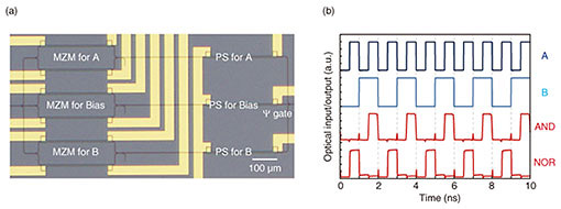
4. Preliminary on-chip integration with PSsTowards practical applications, it is important to show the feasibility of the on-chip integration to demonstrate the phase stability without any optical phase lock loops. Therefore, we also fabricated a Si Ψ gate with several thermo-optic PSs, as shown in Fig. 4(a). For each arm, a pair of a Mach-Zehnder modulator (MZM) and PS are inserted to generate signals A and B, and PBias, ΔΦ and ΔΦBias are adjusted. After conditioning all nine heaters, each MZM was operated with two different frequencies (2 and 1 kbit/s). Then nearly ideal AND and NOR operations with a BC of ~9.5 dB were demonstrated, as shown in Fig. 4(b). All the phase modulators (PMs) should be replaced with other shorter (10–50 µm) and faster (40–100 GHz) PMs [12] to achieve both much lower latency and higher throughput.
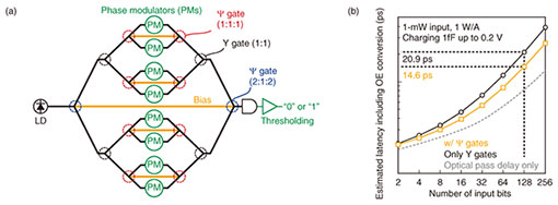
5. Multibit AND circuit by cascading Ψ gatesFigure 5(a) illustrates an optimized multibit AND circuit (8-bit) in terms of latency. In this configuration, we need to use a specific Ψ gate with a 1:1:1 splitting (combining) ratio that enables truly loss-less AND operation (if PA = PB = 1, PBias = 1, ΔΦBias = 0, then Pout = 3, which means no radiation loss) with phase-bit operation (when the digital input is “0” or “1,” the corresponding PM modulates the relative phases ΔΦA and ΔΦB between π (out-of-phase) and 0 (in-phase)). Therefore, all the signal ports connect with PMs directly (no MZMs). However, this phase-bit operation is only available for the first stage because the output of the phase-shift keying operation is not phase bit but amplitude bit. For the intermediate in-phase combining, Y gates are used. At the final stage (and the first splitting stage), the Ψ gates with a 2:1:2 combining (splitting) ratio are optimal for 8-bit operation to minimize insertion loss (note that the optimal ratio for other bit-number operations is different). The combined optical signal is converted by the electrical signal and digitized through a low-latency threshold operator such as a sense amplifier [13]. It should be noted that the BC of the multibit AND operation degrades with the number of the cascade connection. However, the sense amplifier can operate even with a small BC if the absolute output intensity difference between fully matched (all the digital input are “1”) and unmatched (more than one input is “0” etc.) cases is large enough (typically a difference of 10–100 µW is acceptable). Therefore, the BC does not directly limit the feasibility of multibit AND operation. A very similar method was also proposed and demonstrated in CMOS logic circuits based on the current-race method [14]. In the current-race method, the currents from the multiple bit channels (“0” or “1” corresponds to zero or nonzero current output for each bit channel, respectively) are combined through electronic wires, and the combined current is digitized through a sense amplifier. In the case of our photonic method, the signal-combining time can be much shorter than the case of electronics, as we mentioned above. On the other hand, we have an overhead of optoelectric conversion (charging) delay due to the resistance-capacitance time constant of the used photodetector, but this could be drastically mitigated using an ultralow-capacitance (~1 fF) photodetector [15], as discussed in the next paragraph. The computation latency of multibit AND circuits was estimated, as shown in Fig. 5(b). We compared the configurations with and without using Ψ gates and used an ultralow-capacitance photodetector with 1 fF [15]. For instance, the estimated latency for N = 128 (practical level) is ~14.6 ps. The additional charging delay of w/ Ψ gates always becomes half of only Y gates thanks to twice the BC (30% reduction under the same input power of 1 mW). This latency is already 10 times lower than that of the fastest CMOS 128-bit AND circuits [16]. We can also apply wavelength division multiplexing by using more than two input lasers with different wavelengths and corresponding wavelength-selective (resonator-type) electro-optic PMs, further decreasing latency. Although it is also possible to use repeaters for latency compensation, it is no longer energy efficient. The example of this multibit AND circuit application indicates that photonic processing would break the traditional trade-off between latency and energy consumption in CMOS electronics.
6. ConclusionWe experimentally demonstrated ultrashort, simple, integrable, and wavelength insensitive Si wire Ψ gates towards ultralow-latency photonic processing. From the gate length, the minimum computation latency of single logic operation is only ~30 fs, which is more than 100 times lower than that of CMOS electronics. The optical signal loss is also much lower than any other optical gates. The operation function can be switched among XOR, OR, AND, XNOR, NOR, and NAND with a single Ψ gate by tuning input conditions. We also verified the feasibility of on-chip integration for stable operation. Finally, we suggested the original configuration for multibit AND circuits by cascading Ψ and Y gates. By using this configuration, 128-bit AND operation can be carried out at 10 times lower latency than cutting-edge CMOS electronics. Latency can be further lowered by combining with multibit AND circuits and wavelength division multiplexing with a larger number of wavelength channels and by using smaller PMs based on micro rings. We gave an example of logic operations based on linear optical gates. However, linear optical gates can perform specific vector-matrix operations (transformations) without consuming energy. The demonstrated digital-like logic operations are just a specific case of these operations. Therefore, it is expected that low-latency, low-power consumption linear-gate-based vector-matrix operations will be more crucial for photo-electronic-converged artificial-neural-network-accelerator applications [17]. References
|
||||||||||||||||||||||||||||||||||||