|
|||||||||||||
|
|
|||||||||||||
|
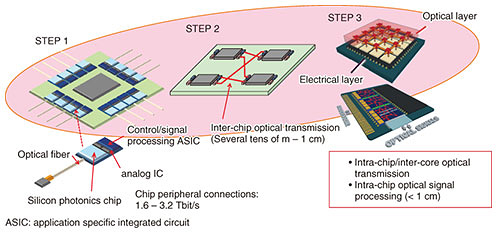
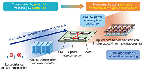
Feature Articles: Disaggregated Computing Will Change the World Vol. 19, No. 7, pp. 58–64, July 2021. https://doi.org/10.53829/ntr202107fa8 Photonics-electronics Convergence Technologies for Disaggregated ComputingAbstractNTT is developing photonics-electronics convergence technologies to implement disaggregated computing. In this article, we describe the concept of photonics-electronics convergence technology, explain the effectiveness of introducing optical technologies into disaggregated computing, and introduce low-power-consumption devices under development. Keywords: IOWN (Innovative Optical and Wireless Network), disaggregated computing, photonics-electronics convergence technology  1. Photonics-electronics convergence technologies supporting IOWN computingAs explained in the Feature Article “Disaggregated Computing, the Basis of IOWN” [1] in this issue, to make the Innovative Optical and Wireless Network (IOWN) a reality, it is necessary to develop computers that can efficiently process a large amount of data, which is incomparable with the past. Photonics-electronics convergence technologies are key to supporting computers that efficiently process large amounts of data. The roadmap for photonics-electronics converged devices is shown in Fig. 1 [2]. STEP 1 involves placing a compact optical module using silicon photonics technology around a central large-scale integrated circuit (LSI). STEP 2 involves placing optical transmission devices, such as semiconductor lasers and photodiodes, in the immediate vicinity of the LSI. STEP 3 involves connecting the LSI chip by optical wiring; as the generation progresses, the size and distance will continue to decrease. In STEP 1, development started targeting communication that connects computers, but as STEP 2 and STEP 3 evolve, the application area will shift to the in-device/in-board interconnect, and it is thought that the introduction of photonics into computers will progress (Fig. 2).
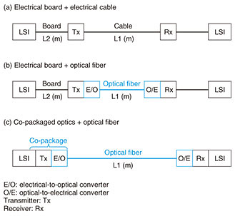
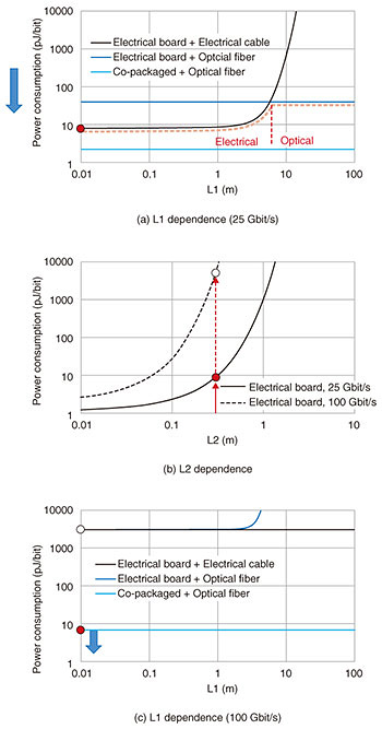
A rack-scale computer connection that is intended for a disaggregated computer requires a transmission distance exceeding several meters. This will be difficult to achieve by electrical connection because of the explosive increase in power due to the increase in speed and distance. The high-speed, high-density, low-power-consumption photonics-electronics converged devices in STEPs 2 and 3 convert electrical signals to optical signals in the vicinity of LSIs, enabling computers with high processing performance to be developed with lower power consumption without being bound by the limitations of electrical transmission. This article describes the photonics-electronics convergence technologies for achieving low power consumption of disaggregated computers. 2. Need for an optical interconnectThis article explains the necessity of using photonics instead of electronics for the connection between boards (printed circuit boards) in a rack and the connection between LSIs on a board using the interconnect model. Figure 3(a) is an electrical model in which an LSI is mounted on a board and a high-speed signal converted from the clock frequency of the LSI is connected to a transmitter on the way through the electrical wiring on the board. It is then received by a receiver formed on the board via a coaxial cable and sent to the LSI. In this case, assume that the length of the cable between the boards is L1 (m) and the wiring length on one board is L2 (m). Figure 3(b) shows the case in which an electrical-to-optical converter is placed after the transmitter to generate an optical signal and an optical fiber is used instead of a coaxial cable. In Fig. 3(c), the transmitter and electrical-to-optical converter are integrated in the same package near the LSI. This configuration is called co-packaged optics (CPO) and corresponds to Figs. 1 and 2.
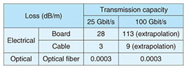
The loss values per unit length when high-speed signals propagate through boards, coaxial cables, and optical fibers are listed in Table 1. For 25-Gbit/s signals (refer to product values), the propagation loss of boards and coaxial cables is larger than that of optical fibers. For example, 3 dB/m for a coaxial cable means that the signal will be –3 dB, or half as large, during 1 m of propagation. Since it is difficult to measure a signal of 100 Gbit/s, an extrapolated value is shown. Various multilevel technologies based on a signal of about 25 Gbit/s (12.5 GHz) per channel are currently used, but the speed limit of CMOS (complementary metal-oxide semiconductor) technology will probably be about 100 Gbit/s in the future. The higher the signal speed, the greater the loss in electrical signal transmission.
Figure 4 shows the results of estimating the relationship between power consumption and distance. The vertical axis in Fig. 4(a) shows the power consumption (mW) divided by the transmission capacity (Gbit/s) (i.e., mW/Gbit/s = pJ/bit) as an index, and the smaller the value, the better the efficiency. The horizontal axis is the length L1 (m) between boards. The calculation result is shown referring to the pluggable transceiver of 25 Gbit/s × 4 channels currently on the market. Comparing the cases in which the electrical cable is used and in which the optical fiber is used, the area where the electrical cable is advantageous and the area where the optical fiber is advantageous are divided at the boundary of 5 m. However, there is a lower limit (red circle) even in the case of the electrical cable. Figure 4(b) shows the relationship between the wiring length L2 (m) on the board and power consumption. This is determined by the power consumption required to transmit L2 = 0.3 m in the curve of 25 Gbit/s. Therefore, if CPO that makes L2 as small as possible are used, efficiency can be further improved, as shown with the sky-blue line in Fig. 4(a).
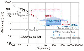
Next, consider the results assuming a transmission capacity of 100 Gbit/s, which will increase transmission speed in the future. As shown with the dotted line at 100 Gbit/s in Fig. 4(b), it is clear that the loss on the board becomes an order of magnitude larger, making the board unusable. Figure 4(c) shows the same estimate as 25 Gbit/s. In the future, power consumption can be reduced as much as possible by opto-electrical conversion in the vicinity of the LSI. When the speed is 100 Gbit/s compared with 25 Gbit/s, the frequency becomes 4 times higher, and the power consumption also increases. There is a need for photonics-electronics converged devices that consume less power while increasing speed. 3. Products and research and development (R&D) trends related to interconnectionIt was shown in the previous section that the applicable areas of photonics and electronics change depending on the signal-transmission distance and speed by using a model. In this model, the case of single channel was explained, but multiple channels are bundled from the side of LSI and used. The higher the shoreline density (Gbit/s/mm), which is the transmission capacity (Gbit/s) per unit side length (mm) of the LSI, the higher the performance. In addition, the lower the power consumption per unit transmission capacity (pJ/bit), the higher the performance. Therefore, the value obtained by dividing the former by the latter, that is, high density/low power consumption = (Gbit/s/mm) / (pJ/bit), is used as the figure of merit. This figure of merit is shown on the vertical axis and distance (m) is shown on the horizontal axis in Fig. 5. When the values of commercial products for interconnection are plotted, although optical interconnection is applied over long distances, the figure of merit is about two orders of magnitude lower than that of electrical interconnection. To improve this figure of merit, low-power-consumption and high-density optical transceivers have been proposed by several R&D institutes. Optical technology, which can be used over a long distance of about 100 m, is expected to be applied to an area of about 10 cm, replacing the electrical area on the board with light. With disaggregated computing, data communication between LSIs and memories, which are limited by the size of physical servers, will be expanded to rack-to-rack scale (several tens of meters). In addition, when higher signal speeds are required, degradation of the figure of merit is predicted for electrical interconnection, so the target is to achieve a range of several centimeters to several tens of meters with a figure of merit equivalent to that of electrical interconnection using optical interconnection.
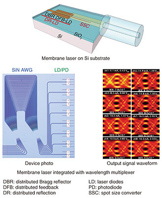
4. R&D on low-power, high-density devices at NTTNTT is researching and developing low-power, high-density optical transmitters and receivers for the aforementioned target areas. The levels reached thus far (transmitter chip) are plotted in Fig. 5 [3]. Among optical transmitters and receivers, semiconductor lasers that convert electrical signals into optical signals are key optical devices. Thin film (membrane) lasers made by NTT are shown in Fig. 6. Vertical cavity surface emitting lasers (VCSELs) are currently the most commonly used semiconductor lasers for short-range optical communications such as board-to-board transmission. Although they have features of low power consumption and low cost, they are not suitable for wavelength division multiplexing technology because of their structure. To increase the communication capacity, high-density integration of single-mode lasers and a wavelength multiplexer is required. Against this background, NTT is developing a membrane directly modulated laser fabricated on a silicon (Si) substrate as a light source for short-range optical interconnects. By fabricating the laser on the Si substrate, the technology of Si photonics, which can produce optical devices such as wavelength multiplexers and photodiodes in high density and at low cost can be applied. By fabricating lasers on the silicon dioxide (SiO2) layer with low refractive index, it is possible to reduce the size and power consumption of lasers by the high interaction between light and injected carriers. We have confirmed 25.8-Gbit/s non-return-to-zero direct modulation operation with energy consumption of 200 fJ/bit, which is comparable to VCSELs [4]. We also demonstrated 8 × 56-Gbit/s PAM-4 (four-level pulse amplitude modulation) operation with integration of an eight-channel directly modulated membrane-laser array and silicon nitride (SiN) arrayed waveguide grating (AWG) multiplexer on Si [5]. We are also developing a laser using photonic crystals to achieve further low power consumption and size reduction [6].
5. Future developmentAs the signal speed and transmission capacity increase, the portion of electrical interconnection is replaced with optical interconnection, and light flows from the rack to the board and even into the board. Therefore, each computer that was previously confined within a physical server becomes a single computer connected at the rack scale. To support this paradigm shift with photonics-electronics convergence technology, we will advance R&D step by step. For photonics-electronics converged devices to be used from communications to information processing, further reductions in power consumption and cost as well as higher density are required. We will attempt to achieve the world of IOWN by applying such devices to future versions of disaggregated computing. References
|
|||||||||||||