|
|||||||||||
|
|
|||||||||||
       |
Feature Articles: Research and Development of Security in the IOWN Era Vol. 20, No. 1, pp. 40–46, Jan. 2022. https://doi.org/10.53829/ntr202201fa7 Cryptographic Circuit Technology Consisting of Optical Logic GatesAbstractWith the progress in nanophotonics, miniature optical devices have been fabricated and the research and development of optical logic gates has become active. We are researching cryptographic circuits consisting of optical logic gates for use in data encryption and authentication in optical computing and optical information communications on the All-Photonics Network, a key element of the Innovative Optical and Wireless Network. In this article, we introduce methods of implementing cryptographic circuits using optical logic gates for the Advanced Encryption Standard, which is one of the de facto standard algorithms. Keywords: All-Photonics Network, optical logic gate, cryptographic circuit
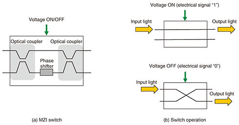
1. Optical computational operations on the All-Photonics Network information-processing platformTargeting the All-Photonics Network (APN) information-processing platform, a key element of the Innovative Optical and Wireless Network (IOWN), we aim to achieve low-power, high-quality, large-capacity, and low-latency information processing by introducing optical technology from the communications network and communications platform up to terminal devices. While data processing on conventional network equipment and computational operations on terminal devices had been executed on electronic circuits, the use of optical technology in such equipment and devices on the APN information-processing platform should improve processing and operation performance. Optical circuits consisting of optical logic gates to enable logical operations constitute one example of optical technology. It has been shown, for example, that optical circuits can be used for the computational operations required by learning algorithms in the field of deep learning and that low-latency and low-power operations can be achieved [1]. 2. Optical cryptographic circuit technologyOn the APN information-processing platform, optical circuits will be used to achieve various types of dedicated hardware to improve computing performance. Therefore, optical circuits will also be used to implement dedicated cryptographic hardware required for ensuring the safety of this platform. It is also desirable for the circuits to be designed to suppress delay and power consumption so that cryptographic operations will not result in overall performance bottleneck. Taking this into account, we have been researching optical cryptographic circuits that can execute encryption and authentication operations by optical signals. In this section, we introduce methods for implementing the Advanced Encryption Standard (AES) by optical circuits. 2.1 AES encryption schemeAES is a block cipher with a 128-bit block length. Key length may be selected from 128, 192, or 256 bits [2]. Here, 128 bits of intermediate values called a “state” are represented by a 4 × 4 matrix with each element consisting of 8 bits. Repeated application of a round function—the basic structure of encryption—to the state outputs the ciphertext. The round function consists of SubBytes, which is a nonlinear operation, ShiftRows and MixColumns, which are linear operations, and AddRoundKey, which combines the state and key. This section focuses on SubBytes and MixColumns as the main operations of AES and introduces methods for achieving these operations by optical circuits. 2.2 Implementing SubBytes by optical logic gatesThe SubBytes operation converts each byte to another byte on the basis of a substitution box (S-box) table determined from specifications. The S-box table is an 8-bit input/output nonlinear conversion. Given a set of 8 bits as input, the operation references the table to obtain an 8-bit output value. For example, the S-box output for an input value of 0xf0 would be 0x8c (input/output values are expressed in hexadecimal numbers). This type of conversion based on a table can be implemented using a Mach-Zehnder interferometer optical switch (MZI switch), which is a type of optical logic gate. As shown in Fig. 1(a), an MZI switch consists of optical couplers and a phase shifter. Applying a voltage to the path embedded in the phase shifter can change the refractive index of the optical waveguide, thus changing the phase difference between the two paths. This enables the MZI switch to operate as a switch that changes the optical pathway. In Fig. 1(b), for example, when inputting light into the upper path and applying a voltage to the path embedded in the phase shifter (corresponding to electrical signal “1”), the optical signal travels straight ahead resulting in output from the upper path. However, when not applying a voltage (corresponding to electrical signal “0”), the optical signal crosses over to the lower path resulting in output from that path.
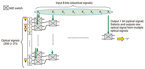
We devised a method for implementing table conversion that outputs a 1-bit optical signal against 8 input bits. This is accomplished by interconnecting a number of MZI switches in accordance with the number of input bits in table conversion and switching paths (Fig. 2). In Fig. 2, the method prepares 256 (= 28) optical signals branched from a single optical source in which each optical signal is set to “light on” (corresponding to an optical signal of bit “1”) or “light off” (corresponding to an optical signal of bit “0”). The method then passes light through the MZI switches while selecting paths in accordance with the 8-bit input (x1, x2, …, x8) and finally selects and outputs one optical signal. This method achieves table conversion that outputs a 1-bit optical signal against an 8-bit input using MZI switches.
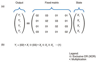
Interconnecting multiple MZI switches, as described above, and appropriately setting the 256 optical signals makes it possible to configure an S-box table. Input to the S-box table is set as MZI input (electrical signals) and output of the S-box table is set as an optical signal. For example, if the least significant bit of each of the 256 values of the S-box table is set as an optical signal, then the least significant bit of the S-box table output with respect to the 8-bit input (x1, x2, …, x8) can be obtained. In the same manner, if the nth bit (n = 1, …, 7) of each of the 256 values of the S-box table output is set as an optical signal, the nth bit of the S-box table output with respect to the 8-bit input can be obtained. To obtain 8 bits of S-box table output, the above processing can be repeated 8 times by time division multiplexing or 8 instances of the circuit in Fig. 2 can be implemented in parallel. For optical signals, it is also possible to calculate 8 bits of S-box table output using only one instance of the circuit in Fig. 2 by multiplexing eight wavelengths and deriving the nth bit of the S-box table for each wavelength. 2.3 Implementing MixColumns by optical logic gatesAs shown in Fig. 3(a), the MixColumns operation is defined as the multiplication of a fixed matrix and the state (where X and Y indicate 8-bit values). On calculating this matrix equation, each 8-bit output can be expressed using Eq. (1) shown in Fig. 3(b) (only Y1 is shown in the figure). Furthermore, in carrying out these multiplications, Eq. (1) can be expressed as five 5-bit exclusive OR (XOR) operations (an XOR operation with 5 input bits and 1 output bit) and three 7-bit XOR operations (an XOR operation with 7 input bits and 1 output bit) [2]. To give an example, we present a method for configuring a 7-bit XOR operation by optical logic gates. A 5-bit XOR operation can be configured in the same manner.
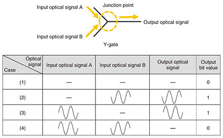
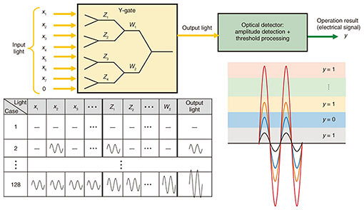
A Y-gate is an optical device that can execute an XOR operation [3]. A Y-gate superposes two input optical signals at a junction point where they meet. An XOR operation or OR operation can be achieved using the property that an optical signal is a “wave” having amplitude and phase, which results in operations approximately 300 times faster than those with electrical logic gates [3]. The principle of an XOR operation by a Y-gate is shown in Fig. 4. This Y-gate inputs two optical signals (input optical signal A and input optical signal B) of equivalent amplitude having a phase difference of 180°. In Fig. 4, “—” indicates a state in which the amplitude of the input optical signal is 0, that is, a state in which there is no input optical signal. These two optical signals are input into the Y-gate and the magnitude of the output optical signal is determined. In case (4) in Fig. 4, for example, the two input optical signals have equivalent amplitude but a phase difference of 180° with the result that the signals cancel each other out, making the amplitude of the output signal 0. Therefore, if we assign bit “0” to the state in which the amplitude is 0 and bit “1” to the state in which the magnitude of the amplitude is essentially the same as that of the input optical signal, an XOR logical operation can be executed, as shown by the bit values of the output optical signal in the figure. In other words, an XOR operation can be achieved using a Y-gate by limiting the two input optical signals to a phase difference of 180°.
However, while executing a 7-bit XOR operation would involve the connecting of multiple Y-gates, taking the results of XOR operations as the input of the next XOR operation means that the phase difference of the two input optical signals of each Y-gate would not necessarily be 180°. (For example, when executing a 4-bit XOR operation (a⊕b⊕c⊕d), the result of the XOR operation between a and b and that between c and d could both be the output of case (2), and those results would then be input to another XOR operation.) There is therefore a need for an operation that can change the phase difference of the two input optical signals to each Y-gate depending on operation results. Such an operation, however, would increase delay and power consumption. To eliminate this need for converting phase during operations, we devised a method that operates on the input to a Y-gate as optical signals having the same phase and corrects the output result by threshold processing at the end of the operations. This method is outlined in Fig. 5. It consists of Y-gate superposition and threshold processing within an optical detector. Y-gate superposition adds up optical-signal amplitudes using a total of 7 Y-gates (since there are 7 input signals, the amplitude of the 8th input is taken to be “0” (light off). Threshold processing, however, uses the fact that the greater the number of optical signals with non-zero amplitudes from among the input optical signals (x1, x2, x3, x4, x5, x6, x7), the larger the amplitude of the output optical signal. It detects the magnitude of this amplitude to determine the output bit. On detecting no output signal (light off) or an amplitude that is an even multiple (2, 4, or 6 times as large) of the amplitude of the input signals, the output result is determined to be bit “0”, and on detecting an amplitude that is an odd multiple (1, 3, 5, or 7 times as large) of the amplitude of the input signals, the output result is determined to be bit “1”. This method enables XOR operations without having to convert the phase of input optical signals at every Y-gate operation. It also enables the processing of Y-gate output to be decreased from 7 times (the number of Y-gate outputs) to 1 time (only at the time of threshold processing).
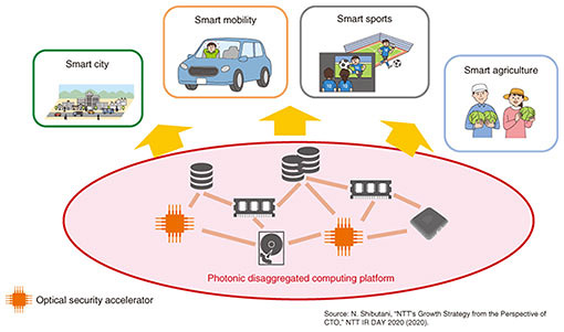
If we let the 7-bit XOR and 5-bit XOR operations calculated from Eq. (1) in Fig. 3(b) correspond to the operation method shown in Fig. 5, one bit of Y1 can be calculated. As with the SubBytes implementations, the calculation of Y1 (8 bits) can be implemented by either of three methods: time division multiplexing, using multiple operation circuits, or multiplexing wavelengths in one operation circuit. 3. Future developmentsWe devised methods for implementing AES encryption circuits using optical logic gates. Going forward, ensuring safety on the APN information-processing platform will require an optical security accelerator that implements security technologies by optical circuits for logical operations, authentication, etc. through a variety of encryption schemes. This type of accelerator is considered a constituent of photonic disaggregated computing [4], a type of architecture supporting the APN information-processing platform shown in Fig. 6. The central processing unit, memory, and other types of devices had been confined to servers, but photonic disaggregated computing is a new architecture that can be treated as computers on a rack or a datacenter scale by connecting and distributing those devices over a high-speed optical network. An optical security accelerator will lead to a safe photonic disaggregated computing platform and the provision of safe smart services on that platform. To achieve a low-latency and low-power optical security accelerator, we will continue our research on new schemes for implementing encryption and authentication processes by taking advantage of optical characteristics. Therefore, we wish to contribute to the deployment of a safe IOWN.
References
|
||||||||||