|
|||||||||
|
|
|||||||||
       |
Feature Articles: The Forefront of Nanomechanics Research Vol. 20, No. 4, pp. 54–58, Apr. 2022. https://doi.org/10.53829/ntr202204fa9 Highly Sensitive Detection and Control of a Nanowire Mechanical Resonator Using an Optical MicrocavityAbstractSemiconductor nanowires have a rod-like structure that is too thin to be seen by the naked eye. This fine structure strongly confines photons and electrons, enabling us to use quantum nano-optoelectric properties to control photons and electrons individually. Semiconductor nanowires also function as nanomechanical resonators when their flexural motion is available. To achieve new opto-electro-mechanical hybrid quantum devices, NTT laboratories have developed technology to detect and control nanowire mechanical motion with high sensitivity. Keywords: optical microcavity, nanowire, mechanical resonator
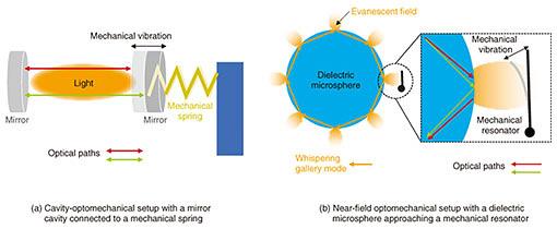
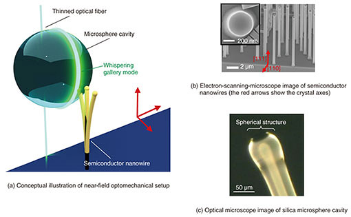
1. Semiconductor nanowire as hybrid mechanical deviceA semiconductor nanowire is a very thin rod with diameters of hundreds of nanometers (about 1/100 the width of a strand of hair) and lengths of a few micrometers. If you compare a semiconductor chip of a few millimeters square to the size of a tennis court, a nanowire would look like a toothpick standing upright on the court. Therefore, it is difficult to see the whole picture with a light microscope as well as with the naked eye. Even with such a small structure, it is possible to confine photons and electrons inside it using the latest semiconductor technology. NTT laboratories are conducting basic research for the application of semiconductor nanowires to optical and electronic devices such as ultralow-power semiconductor lasers and spintronics devices capable of controlling electron spin. In addition to such quantum optoelectric properties, semiconductor nanowires have the functions of nanomechanical devices with excellent mechanical properties. For example, a nanowire grown perpendicular to a substrate can be used as a nanomechanical resonator because it shows resonant flexural motion. Since this nanomechanical resonator has a very small structure, its vibration characteristics are significantly modified by external forces and additional mass due to adhesion of small objects on the resonator. By using this ultrasensitive feature, a nanomechanical resonator can be used as a mechanical sensor to detect external forces and nano/micro particles by reading the changes in its vibration characteristics. It can also be utilized as a mechanical actuator driven by light or electricity. Thus, various studies have investigated the characteristics of nanowires used as nanomechanical resonators [1]. Attempts to develop a hybrid device with optical, electrical, and mechanical properties, using a semiconductor nanowire have just begun. Such innovative hybrid devices would enable us to implement new information processing using a combination of optical, electrical, and vibration signals, and control optical and electrical material properties with vibration. Bringing them into an extreme region, where quantum mechanical properties of photons, electrons, and phonons appear, will accelerate the quantum information technology through the development of novel quantum light sources and quantum memories. Such hybridation will pave the way to creating innovative quantum opto-electro-mechanical devices [2]. Although semiconductor nanowires are strong candidates for developing such a hybrid quantum device, the technology for detecting and controlling tiny mechanical vibrations has not been sufficiently developed. The main issue originates from the size of the nanowires, which are too small to be seen directly. The conventional laser-irradiation technique, which is used to detect vibrations in solid-state nanomechanical devices that are barely visible, is not suitable to resolve a nanowire structure smaller than the wavelength of light (about 1 µm). Therefore, we need to develop new and effective methods for detecting and controlling extremely small nanowire mechanical motion. The following is a brief introduction to near-field cavity optomechanics, which was recently developed by NTT laboratories using a small glass sphere as a new technology for ultrasensitive vibration detection and control of semiconductor nanowires [3]. 2. Near-field optomechanics using a glass microsphere cavityThe mechanism of cavity optomechanics can be understood in a model of a mirror cavity with one side connected to a mechanical spring, as shown in Fig. 1(a). The cavity is a box that strongly confines light. In this model, light is confined by reflection back and forth between two mirrors. When the mechanical spring attached to the mirror vibrates, the path of light confined in the cavity changes. Since light has the properties of a wave, this path change is represented by a change in the optical phase of the wave. By reading this optical-phase change, vibration of the mechanical spring can be detected with high sensitivity. When light strongly confined in the cavity is reflected by the mirror, however, a force is applied to the mirror as a backaction that changes the momentum of the light. This force (radiation pressure) can be used to drive mechanical springs and control their resonance frequency. The radiation pressure of light was discovered in the tail of a comet in ancient times, but it was not until the early 2000s that cavity optomechanics flourished as an applied technology. State-of-the-art optomechanical devices have successfully detected and controlled quantum fluctuations corresponding to a single vibrating quantum particle (i.e., a single phonon). However, applying such cavity optomechanics to semiconductor nanowires, which are extremely small structures, is difficult. This is because it is not easy to fabricate nanowires produced using special growth techniques and high-quality optical cavities on the same chip. Even if large cavities such as mirror cavities are installed externally, it is difficult to generate sufficient optomechanical coupling to such small nanowires. We demonstrated, for the first time, near-field optomechanics with a microsphere approaching semiconductor nanowires. The optical microsphere cavity, the key to this technology, is fabricated independently of semiconductor nanowires by processing transparent glass called silica glass, which is also a well-known material for optical fibers. Just as glassworkers make glass cups and wind chimes, very small glass balls of several tens of micrometers in diameter can be made by heating and inflating the tips of silica optical fibers. When a thinned optical fiber is brought into contact with this glass ball, a cavity-optical mode called the whispering gallery mode is induced in which light leaked from the optical fiber circularly travels across the glass ball’s surface. In this case, as shown in Fig. 1(b), there is an evanescent field with finite optical leakage to the outside of the sphere due to the total reflection. When the evanescent field is brought close to the nanowire, the path of the light (i.e., optical phase) around the cavity changes in response to the nanowire vibration. This change in the optical phase makes it possible to detect the vibration. As in the mirror cavity example, this induces backaction forces to the nanowires. By using this interaction between light and mechanical motion, nanowire mechanical motion can be controlled by laser light. This near-field cavity-optomechanical technique with the optical evanescent field enables highly sensitive detection and control of nanowire vibrations smaller than the wavelength of light.
The experimental setup is depicted in Fig. 2(a). The measurement uses one of the InAs/InP (indium arsenide/indium phosphide) heterostructure semiconductor nanowires (14-µm long, 500 nm in diameter; Fig. 2(b)) grown in great numbers on an InP substrate. The optical cavity is a 40-µm-diameter glass ball fabricated via electrical discharge processing on an optical fiber tip (Fig. 2(c)). The whispering gallery mode is induced by contacting a communications-wavelength optical fiber thinned to about 1 µm with the glass ball. By bringing the evanescent field of this mode close to the nanowire, we observed an optical resonance with a quality (Q) factor of 1.8 × 10⁵. The Q factor is a quality measure of how strongly light can be confined in the cavity, and 105 refers to highly confined optical resonance classified as having a high Q factor.
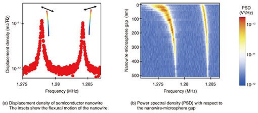
3. Sensitive displacement measurement and vibration control of semiconductor nanowiresWe constructed an optical measurement system called a homodyne optical interferometer to read out the change in the phase of light accompanied by the nanowire vibration with high sensitivity. The advantage of this interferometer is that the phase change of the light can be read with high sensitivity, which is different from the usual detection method for detecting optical power. When spectral measurements were carried out on the interferometer output signal, two peaks were observed near 1 MHz (Fig. 3(a)). These peaks correspond to the thermal fluctuations of the nanowire mechanical modes in both the vertical and horizontal directions. Thermal fluctuations are vibrations in which the nanowires move randomly depending on the ambient temperature, and the higher the temperature, the greater the fluctuation. The thermal fluctuation of the nanowires used in this experiment at room temperature was about 100 pm (~ 1 × 10–11 m/Hz0.5, which is the same size as one atom), and the minimum detectable displacement (corresponding to the floor level in Fig. 3(a)) was found to be about 10 pm. This minimum detectable displacement corresponds to the amount of thermal fluctuation expected when the nanowires are placed in an environment of 2.8 K. This indicates that the nanowire-thermal fluctuation can be detected even in a very low temperature environment of about –270°C, which is near absolute 0. In such a cryogenic environment, electrons confined in semiconductor nanowires exhibit quantum mechanical properties. Therefore, if we can extract the mechanical freedom of nanowires in such an environment, we will make great progress toward hybrid quantum devices. It is important not only to detect vibrations but also to develop technologies to actively control them. Our technique based on near-field cavity optomechanics with a small glass sphere can detect the vibration of the nanowire and simultaneously control the vibration with laser light. This is the same principle as the optical gradient force applied in optical tweezers. The force acts on the object from the lower to higher density of the optical electric field. This force increases as the gap between the cavity and nanowire decreases, causing a change in vibration frequency and increase in linewidth (Fig. 3(b)). We have also succeeded in using this force to rotate the vibration axis of the nanowires, although the details are omitted here. Therefore, we found that the vibration characteristics of nanowires can be precisely controlled using the strong optical gradient force in the microsphere cavity.
4. Future prospectsThe technology introduced in this article enables highly sensitive detection and control of mechanical motion in semiconductor nanowires that are smaller than the wavelength of light. The detection sensitivity is expected to be further enhanced by improving the Q factor of the optical cavity. The Q factor of the optical cavity used in the above experiment was about 105, but it is also possible to obtain a Q factor of 107 or more by machining with better accuracy. It has been theoretically predicted that such a high Q factor can increase the detection sensitivity to the level of not only thermal fluctuations but also quantum-mechanical fluctuations, which are two orders of magnitude smaller than thermal ones. Although there are still many problems to be solved experimentally, we will continue our research on semiconductor nanowires for innovative hybrid quantum devices. References
|
||||||||