 |
|||||||||||||||||||||||||||||||||||||
|
|
|||||||||||||||||||||||||||||||||||||
|
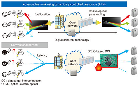
Regular Articles Vol. 20, No. 4, pp. 65–73, Apr. 2022. https://doi.org/10.53829/ntr202204ra1 High-speed Tunable Laser Based on Electro-optic Effect for Wavelength SwitchingAbstractWe developed a high-speed tunable laser, the lasing wavelength of which is tuned by the electro-optic (EO) effect of a semiconductor multi-quantum well. The laser exhibited a tuning range of 35 nm (full C-band), which is the world’s first of an electro-optically tunable laser. Thanks to the low-thermal generation and high-speed response of the EO effect, we also achieved less-than-30-mW tuning-power dissipation and sub-nanosecond wavelength switching. The laser also showed a linewidth of less than 350 kHz, which is acceptable for conventional digital coherent systems. We also demonstrated unprecedented high-speed wavelength switching for 128-Gbit/s coherent signals with this laser, which will contribute to the All-Photonics Network. Keywords: tunable laser, high-speed wavelength switching, electro-optic effect 1. IntroductionA high-speed tunable laser diode (TLD) is key to dynamic allocation of wavelength (λ) resources to individual network units (Fig. 1) in our All-Photonics Network (APN) [1]. Since the motivations of this future network are lowering the latency and power consumption of conventional electronic-based network units [2, 3], TLDs are required to be tuned with high-speed and lower power dissipation. Low-noise operation of the laser, i.e., narrow-linewidth performance, is also important to ensure communication capacity by using higher modulation formats with digital coherent technology. In addition to an evolving optical network architecture, TLDs are also beneficial to remote-sensing systems such as those using tunable diode laser absorption spectroscopy [4, 5] and light detection and ranging (LiDAR). For example, the tuning λ-range, tuning speed, and linewidth of a TLD correspond to the beam steering range, scan speed, and detection distance, respectively, in a non-mechanical-type LiDAR system based on coherent detection.
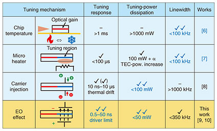
While such high-performance TLDs are indispensable for future optical communication/remote-sensing systems, conventional tuning mechanisms face performance limits (Table 1). Laser-chip temperature control (an industry-successful tuning approach [6]) using a thermoelectric controller (TEC) has a poor tuning speed and Watt-class tuning-power dissipation. Although using the thermo-optic (TO) effect with a micro heater [7] is a suitable approach for lowering the tuning power to ~100 mW, the tuning response is limited to a few microseconds, which is not fast enough for the above-mentioned future network systems, which will require a nanosecond-order response in λ-switching. Carrier-injection into a laser cavity [8] is suitable for low tuning power and high-speed tuning; however, linewidth broadening due to the free-carrier-induced noise cannot be avoided.
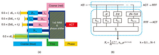
Therefore, we focused on using the electro-optic (EO) effect as the tuning mechanism of a TLD [9, 10]. The small current generated during EO tuning is beneficial to low-tuning-power dissipation. In addition, the tuning speed is very high since the response depends only on the intrinsic capacitance of the laser cavity, unlike the microsecond-order TO effect using a micro heater. The depletion cavity under a voltage bias used for EO operation is also suitable for narrow-linewidth laser operation, which is difficult for carrier-injection-type TLDs. However, a fatal disadvantage of the EO effect is the small reflective index change (Δn). Even with the quantum-confined Stark effect (QCSE) of a semiconductor multi-quantum well (MQW), which is a type of EO effect with a relatively large Δn compared with other EO effects, the Δn is typically about 10% of the TO and carrier effect. This means that the tuning range of an EO-tunable laser results in an impractical tuning range that is ~10% those of conventional TLDs. To use the EO effect for a TLD while overcoming the impractical Δn, we use a reflection-type transversal filter (RTF) [11, 12] as a tunable filter in a TLD cavity. The advantage of an RTF is that we can design the filter tunability (the filter-spectral shift for a given Δn of the waveguide) while tunabilities of conventional filters depend only on the filter-waveguide material. In other words, we can use the EO effect for a TLD with a practical tuning range by compensating for the small Δn of the EO effect with the large tunability of the RTF. In this article, we discuss the design and present the experimental results of a newly developed EO RTF laser. It exhibits a less-than-30-mW tuning-power dissipation and sub-nanosecond λ-switching with a practical 35-nm tuning range. The laser linewidth is less than 350 kHz, which is acceptable for conventional digital coherent systems. We also discuss the unprecedented high-speed λ-switching for coherent 128-Gbit/s signals with this laser. 2. DesignFigure 2(a) shows a schematic of our RTF laser that consists of an active optical gain (ACT) and RTF for a lasing-wavelength selector. An RTF is an optical-region finite impulse response (FIR) filter, the tap coefficients of which are designed so that the filter has a required spectrum. Namely, signals input into a filter (x(t)) are sampled with a time interval, Δt, and each sampled signal is multiplied by a corresponding tap coefficient (hm,k). They are then summed with a summation circuit. The system transfer function Xk is shown in Fig. 2(b). We express the transversal structure of the FIR shown in Fig. 2(b) with a 1x5 multi-mode interference coupler (MMI) and reflection-type delay lines. Note that the factor 0.5 of each delay-line length in Fig. 2(a) comes from light making a round-trip in the line. Therefore, this factor vanishes when we consider the corresponding optical path. When signals (broad-band light from the ACT) are input into the RTF, the 1x5 MMI functions as a signal sampler. It also functions as a summation circuit; therefore, the signal (spectrally filtered light) returns to the input port (ACT). When
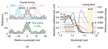
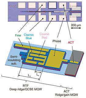
We define Le as a unit tuning electro-length and install electrodes with lengths of iLe or (5–i)Le on a delay line with idLc, as shown in Fig. 2(a). These electrodes are then used for the red and blue shifts of the coarse filter spectrum. The wavelength shift Δλ is shown as follows [9]. where Γ is an optical confinement factor in the MQW of the RTF delay line. We assume Γ = 0.5 in our waveguide. This relation is introduced by the RTF transfer function. The fine-tuning efficiency is also expressed with a similar expression involving Since we intend to tune the RTF spectrum with the QCSE, we need to know the Δn to determine Le. Figure 3(b) shows a theoretical Δn derived from the QCSE of our InAlGaAs/InAlAs (indium aluminum gallium arsenide/indium aluminum arsenide) MQW calculated on the basis of k・p perturbation theory [4, 13]. It was found that the Δn of our MQW is ~0.003. Using the Δn and Eq. 1, we determined Le to be 180 μm for Δλ = 0.5 × 35 nm. The 35 nm is the C-band range and the factor 0.5 in the Δλ expression comes from the fact that we can use red and blue shifts for the coarse tuning.
3. Laser performanceFigure 4 shows a photograph of our fabricated RTF laser and corresponding schematic of the waveguide structure. The ACT has a ridge waveguide structure and made of an InGaAsP (indium gallium arsenide phosphide) MQW with optical gain in the 1.55-μm-wavelength band. The RTF has a deep-ridge structure and made of an InAlGaAs MQW for the QCSE. After we grow the QCSE MQW on an InP (indium phosphide) wafer, we partially replace the MQW with the active MQW by butt-joint regrowth [14]. After preparing the wafer, we form the ACT and RTF waveguides by dry etching and evaporate electrodes on the RTF and ACT with an electron beam evaporator. While the laser has a deep-ridge structure, we use no resin such as Benzocyclobutene for the planarization in the wafer process to suppress external stress on the waveguide [15].
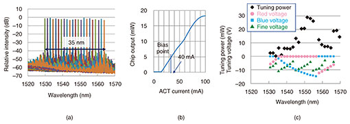
Figure 5(a) shows the lasing spectra of a fabricated RTF laser. All experimental results shown in this article were obtained with an injection current into an ACT of 40 mA (~6-mW output as shown in Fig. 5(b)) and chip temperature of 45°C. We confirmed a 35-nm tuning range (full C-band) for the laser with over 40-dB side mode suppression ratios by applying tuning voltages to four electrodes. The tuning voltages, except for the phase electrode, are as shown in Fig. 5(c). Phase-tuning voltages were also adjusted so that the lasing wavelengths matched the International Telecommunication Union - Telecommunication Standardization Sector (ITU-T) grid [16]. We believe that this is the world’s first report of an EO-tunable laser with a practical tuning range. Figure 5(c) also displays the corresponding tuning-power dissipation defined as the total product of the applied tuning voltages and corresponding photocurrents. We believe that the obtained less-than-30-mW tuning power is remarkably low compared with conventional TLDs. It should be noted that most of the 30 mW comes from the increase in the electrostatic energy of the photocurrents in the depletion layer rather than thermal energy. Therefore, the tuning-power dissipation of the RTF laser hardly increases the chip temperature, resulting in little effect on TEC power dissipation. This is also beneficial in terms of the small λ-drift in λ-switching described below.
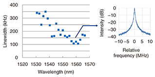
In Fig. 6, laser linewidths measured using the delayed self-heterodyne (DSH) method are also plotted. We observed linewidths of less than 350 kHz, which is acceptable for conventional digital coherent technology, indicating the advantage of having a laser-depletion cavity under EO tuning.
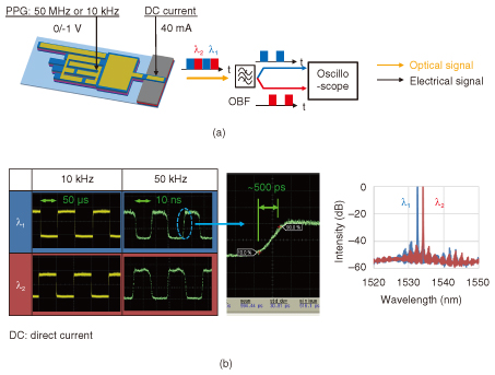
We also measured the tuning response of the RTF laser (Fig. 7). We applied 50-MHz and 10-kHz square pulses to the RTF laser using a pulse-pattern generator (PPG) and selected a target λ with an optical bandpass filter (OBF). Thanks to the high-speed response of the EO effect, the laser showed a record sub-nanosecond λ-switching time. In addition to the fast response, we confirmed that the response waveforms hardly changed even for 10-kHz modulation. This indicates that there was little λ-drift due to the slow thermal effect during dynamic tuning, which occurs for carrier injection-type TLDs. Although the experiment was rough for evaluating the dynamic wavelength, we also conducted a more detailed measurement using a chirp analyzer and obtained the same conclusion [17]. This dynamically stable performance is practically important to simplify the control electronics in optical switching with burst signals described in the next section and in sensing with adaptive tuning speeds, such as for foveated imaging using a swept light source [18].
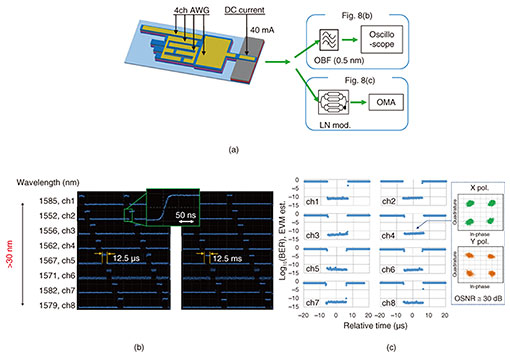
4. Eight-channel λ-switching for 128-Gbit/s coherent signalsWe demonstrated eight-channel λ-switching to prove the feasibility of our RTF laser for optical switching light sources. Figure 8(a) shows the experimental setup. We used a four-channel arbitrary waveform generator (AWG) instead of the PPG used in the experiment shown in Fig. 7(a). As shown in Fig. 8(b), we achieved random eight-channel λ-switching with a response time of ~30 ns (AWG bandwidth limit). The important point is that we obtained the same waveform for pulse widths of 12.5 μs and 12.5 ms, which differ by 1000 times. This is a predictable result from the 10-kHz monotonic pulse-modulation experiment shown in Fig. 7(a). This RTF laser is also burst tolerant in addition to having a high-speed tuning response. Finally, we input the λ-switched laser into a commercial lithium niobate (LN) in-phase and quadrature (IQ) modulator. The laser was modulated with 32-GBd dual polarization quadrature phase shift keying via the IQ modulator and detected with an optical modulation analyzer (OMA). As shown in Fig. 8(c), we confirmed dynamic bit error rates (BERs) of less than 10-10 in all eight λ-channels, which indicates that the RTF laser has a practically narrow linewidth for a coherent format in addition to high-speed and burst-tolerant characteristics. We believe that the above demonstration results reflect the unique performance of the EO RTF laser.
5. ConclusionWe described the design, basic laser characteristics, and λ-switching demonstration of a newly developed EO RTF laser. The laser has unique characteristics thanks to the excellent EO effect used as the tuning mechanism. We believe that the laser will contribute to future optical networks such as the APN and high-function remote sensing systems using dynamically controlled laser wavelengths. References
|
|||||||||||||||||||||||||||||||||||||


