|
|||||||||||||||||||||||||||||||||||||
|
|
|||||||||||||||||||||||||||||||||||||
       |
Feature Articles: Optical and Wireless Transmission Technologies for IOWN/6G Vol. 20, No. 7, pp. 17–23, July 2022. https://doi.org/10.53829/ntr202207fa2 Future Development of Digital Coherent Optical Transmission TechnologyAbstractDigital coherent optical transmission technology—which digitally incorporates physical quantities such as amplitude, phase, and polarization and maximizes transmission performance through advanced signal processing—is the latest generation of optical transmission technology; however, the technology must be further developed to implement the Innovative Optical and Wireless Network (IOWN). The latest trends and future development of digital coherent optical transmission technology are described in this article from the perspectives of high-speed and high-capacity transmission, low-power devices, and software-based autonomous control. Keywords: optical transmission technology, digital coherent, All-Photonics Network
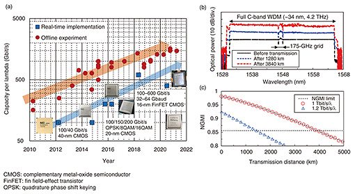
1. IntroductionSince the dawn of the Internet, Internet traffic has continued to grow exponentially in Japan and around the world as various services emerge and spread. To support this growth in traffic, optical-fiber transmission technology has continued to evolve generationally through the introduction of new technologies such as wavelength division multiplexing and optical-amplification relay. The latest generation of these technologies is digital coherent optical transmission technology, which captures all the physical quantities of light (i.e., polarization, amplitude, and phase) as digital data and compensates for distortions in optical-fiber transmission lines and optoelectronic devices through advanced signal processing [1]. To implement the Innovative Optical and Wireless Network (IOWN), which aims to integrate the real and virtual worlds into a rich society that embraces diversity, optical transmission technology must also evolve to provide even higher capacity, lower power consumption, and higher functionality. The latest trends and future development of digital coherent optical transmission technology are introduced in terms of high-speed and high-capacity transmission, compact and low-power devices, and software-based autonomous control. 2. Initiatives concerning further increase in speed and capacityThe expansion of communications within and between datacenters and the penetration of applications such as on-demand video streaming and cloud computing have further increased the demand for optical transmission with higher capacity. Regarding high-capacity networks, capacity per wavelength channel must be increased before the network can be built economically. Evolution of optical transmission capacity per wavelength channel in the cases of offline experiments and in commercial systems is shown in Fig. 1(a). High-capacity transmission exceeding 1 Tbit/s per wavelength has been experimentally demonstrated. In these demonstrations, modulation speed significantly increased and modulation schemes with higher modulation levels/high-order modulated signals were introduced. The modulation speed in the first generation of digital coherent optical transmission (100 Gbit/s per wavelength) was 32 Gbaud, but it has increased to 100 Gbaud and higher [2, 3]. This increased modulation speed was a result of increasing the speed of analog components such as analog-to-digital converters (ADCs) and digital-to-analog converters (DACs), optical modulators, drivers, photodiodes, and transimpedance amplifiers [4–6]. Probabilistic constellation shaping (PCS) [7], which can achieve a capacity close to the Shannon limit, has attracted attention and is used together with quadrature amplitude modulation (QAM) composed of 64 or more constellation points. Signal distortion caused by analog components in the transmitter and receiver is a major issue in regard to increasing the capacity of optical transmission systems. As the symbol rate increases and the multi-modulation level becomes higher, signal distortions are caused by frequency-bandwidth limitation and crosstalk in the analog components and the electrical wiring in printed circuit boards and other components. These distortions are compensated for by setting optimal filter coefficients, which are estimated by calibration, for each digital equalization filter (i.e., one for transmission and one for reception). NTT Network Innovation Laboratories is developing technology to compensate for such waveform distortion with high accuracy. There are two problems with digital estimation: (i) increasing the peak-to-average power ratio and lowering signal quality [8] and (ii) tracking the time variation of waveform distortion due to operating temperature, age deterioration, and control dither. To ensure sufficient transmission performance, it is important to divide the roles of sender-side pre-equalization and receiver-side equalization. By applying our research and development (R&D) technologies to address these issues, we have commercialized an application-specific integrated circuit that achieves digital coherent transmission at a rate of up to 600 Gbit/s [9]. Regarding the development of a next-generation optical transmission system, NTT Network Innovation Laboratories has further increased modulation speed to 168 Gbaud and experimentally demonstrated transmissions of a 1-Tbit/s light signal over 3840 km and of 1.2-Tbit/s light signal over 1280 km [2]. We achieved these high modulation speeds by using two analog multiplexer (AMUX) front-end integrated modules [5], which respectively use polarization-multiplexed PCS-16QAM and 36QAM modulation schemes. This light signal is wavelength-division multiplexed (WDM) with optical frequency spacing of 175 GHz. The spectrum of the WDM signal before and after transmission is shown in Fig. 1(b). The transmission line consists of pure-silica-core fiber with an 80-km optical-amplification relay section and uses both backward-pumping distributed Raman amplification and erbium-doped-fiber amplification. Each amplification achieves spectral-utilization efficiencies of 5.71 and 6.85 bit/s/Hz, respectively. Measured dependence of normal generalized mutual information (NGMI) on transmission distance for 1-Tbit/s and 1.2-Tbit/s signals is shown in Fig. 1(c). As shown in the figure, NGMI values were above 0.857, namely, error-correction threshold for 21% redundancy level, for the 1-Tbit/s signal after 3840-km transmission and for the 1.2-Tbit/s signal after 1280-km transmission. This result indicates that error-free transmission is possible. Note that in this experimental demonstration, we only used the C-band, but we are conducting R&D with the aim of expanding the bandwidth to the L- and S-bands.
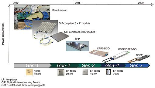
3. Initiatives concerning miniaturization and power reductionTo handle ever-increasing communication traffic, optical networks must be able to continuously increase capacity. However, the installation space and power supply of optical transmission equipment are limited; accordingly, achieving higher capacity necessitates smaller, lower-power optical interfaces. Since miniaturization of devices lowers their heat-dissipation performance, low power consumption as well as miniaturization and high-density mounting of the devices that configure the optical interface are key factors in achieving miniaturization. It is therefore essential to reduce the power consumption of a digital signal processor (DSP) because it accounts for a large portion of the power consumption of optical interfaces. Digital coherent optical transmission technology was first implemented in long-distance transmission systems configuring the backbone networks of telecommunications carriers. As the technology has matured, miniaturization, power reduction, and cost reduction have progressed, and the technology has become more widely used in short-distance transmission systems such as metro networks and datacenter-interconnect (DCI) networks. This technology is expected to be applied to access networks and networks within datacenters in the future. Low-power technologies will also become increasingly important in regard to creating future massively multi-parallel, high-capacity optical transmission systems using multicore fibers with spatial multiplexing. The progress in miniaturization and power reduction of coherent transceivers is shown in Fig. 2. The DSPs developed and practically applied at NTT laboratories, i.e., installed in a coherent transceiver, are shown below the horizontal axis. Coherent transceivers are mainly used for metro and DCI networks, and their miniaturization and power-consumption reduction are rapidly progressing in a similar manner to low-power DSPs. Currently, 400-Gbit/s pluggable transceivers, such as the C form-factor pluggable 2 digital coherent optics (CFP2-DCO) and quad small form-factor pluggable double density (QSFP-DD), are in practical use.
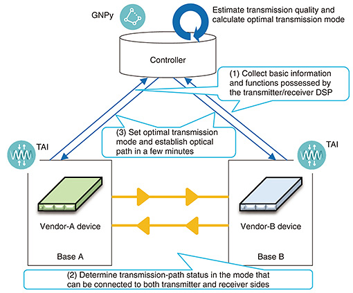
DSPs for optical communication are required to operate at extremely high speeds and low power consumption, so the state-of-the-art complementary metal-oxide semiconductor (CMOS) process is always applied to reduce power consumption. However, this power consumption cannot be reduced sufficiently by improving the CMOS process. Accordingly, application of new signal-processing algorithms, selection of functions in accordance with application [10], and optimization of performance have progressed in regard to functions such as reduction in the digital sampling rate, wavelength-dispersion compensation, adaptive equalization, and forward-error correction (FEC). Although the application of state-of-the-art CMOS processes and innovations in signal-processing algorithms have significantly reduced the power consumption of digital circuits, the power consumption of analog circuits, such as DACs and ADCs, has not yet been significantly reduced, partly due to the effect of the higher transmission and reception signal speeds of those circuits. For that reason, the power consumption of analog circuits accounts for a larger percentage of the total power consumption in each generation of DSP, and one of the major challenges for further power reduction is to reduce the power consumption of analog circuits. With the aim of achieving further miniaturization and lower power consumption, co-package mounting technology, in which a DSP and silicon-photonics-based optical transmitter-receiver device called coherent optical subassembly (COSA) [11] are mounted in a single package, has been researched and developed. High-density mounting of the DSP and COSA enables significant miniaturization, while shortening the high-speed analog electrical wiring between the DSP and COSA minimizes losses and keeps signal drive power low. To implement the future IOWN-based All-Photonics Network, we are conducting R&D aimed at drastically reducing power consumption by offloading functions that are currently executed by digital signal processing to optical processing. NTT Network Innovation Laboratories has demonstrated a significant improvement in optical signal-to-noise ratio (SNR) tolerance for 800-Gbit/s-class optical transmission by compensating for signal-waveform distortion caused by the bandwidth characteristics of the optical transmitter and receiver in conjunction with digital signal processing and optical processing [12]. This performance improvement makes it possible to simplify digital signal processing, thus reduce the power consumption of the DSP. 4. Initiatives concerning automated control using softwareSoftware-defined wide-area network (SD-WAN) technology, which separates the physical network and device hardware from their control planes and manages them using software, has been commercially introduced in the market for forwarding equipment such as routers, and a system that connects remote-user sites and enables centralized control using software is now in place. In the era of full-fledged IOWN, user terminals equipped with various transmission functions, such as routers with coherent modules and white-box switches, will become increasingly popular. To connect these terminals while attaining low latency and low power consumption by reducing the number of optical-electrical conversions, using direct connection via a carrier network is being considered [13], and it is expected that software-based automatic-configuration technology for optical transmission networks will be implemented. However, for optical transmission below layer 1, complex physical factors such as wavelength dependence of optical amplifiers and nonlinear optical effects in fiber have been considered a barrier to automated control using software as in the case of SD-WANs. To dynamically connect arbitrary user ends, a new method for quickly estimating transmission-path characteristics that determine transmission distance and capacity of optical transmission networks and real-time measurement of transmission quality using receivers are required. The Open Optical & Packet Transport project group of the Telecom Infra Project [14], which aims to define open technologies, architectures, and interfaces in optical and Internet protocol networking, is developing GNPy [15], an open-transmission-path design tool based on transmission-quality estimation using Gaussian-noise models, and a transponder abstraction interface (TAI) [16], which separates the hardware and software of a transponder. NTT Network Innovation Laboratories is contributing to openness in these areas and aims to implement a technology that automatically optimizes the transmission mode of optical paths between different vendors and devices and establishes optical-path connections in a short time by using open interfaces and tools such as a TAI and GNPy (Fig. 3).
Manual work has traditionally been required to connect such optical paths, and the process from service order to optical-path connection took a long time, ranging from several days to several weeks. As schemes for digital coherent optical transmission become more sophisticated and transmission modes become more diverse, the design and coordination of optical paths are becoming more complex. Our developed technology calculates the optimal transmission mode (modulation scheme and FEC type)—even in an environment in which multi-vendor transmission equipment has been deployed—by collecting such information via a TAI and estimating transmission-path conditions and transmission quality by means of GNPy and other methods. Moreover, by setting that information to the transmitter and receiver DSPs, an optical-path connection is established in a few minutes [17]. Specifically, these procedures/processes are carried out with the following sequence of steps. (1) The basic information and functions possessed by the transmitter and receiver DSPs (configurable modulation scheme, FEC type, etc.) are collected via the TAI, and the optical-path connection is established after setting a transmission mode that can be connected to both the transmitter and receiver. (2) Via step (1), parameters, such as bit error rate and wavelength dispersion, are collected from the receiver DSP, and the quality of the transmission channel is estimated. From these parameters, the optimal transmission mode is calculated—with appropriate margin settings—on the basis of geometric SNR estimated by GNPy. (3) On the basis of the calculated transmission mode, parameters such as modulation method and FEC type for the transmitter and receiver DSPs are set, and an optical path between transmission devices of different vendors is opened in a few minutes. 5. Concluding remarksTo implement optical transmission technology that supports IOWN, NTT Network Innovation Laboratories will research and develop digital coherent optical transmission technology from the viewpoints of high-speed and large-capacity transmission, low-power devices, and software-based autonomous control. References
|
||||||||||||||||||||||||||||||||||||