 |
|||||||||||||||||||||
|
|
|||||||||||||||||||||
       |
Front-line Researchers Vol. 21, No. 11, pp. 6–12, Nov. 2023. https://doi.org/10.53829/ntr202311fr1  Taking the Challenge to Create Novel
|
||||||||||||||||||||
 |
 |
Creating and discovering new materials by using high-quality complex-oxide-thin-film growth technology
—Could you tell us about your current research?
My research theme focuses on creating new materials and elucidating their physical properties. In the three years since my last interview for “Front-line Researchers,” our research team made three main accomplishments: (i) discovery of a new copper oxide (cuprate) superconductor through the formation of artificial superlattices; (ii) development of a pioneering and efficient method for growing high-quality thin films; and (iii) substantiation of a magnetic Weyl semimetal state in SrRuO3 (Sr: strontium, Ru: ruthenium, O: oxygen) by using ultra-high-quality thin films.
I’ll explain the first accomplishment, discovery of a new cuprate superconductor, in more detail. Superconductivity is a phenomenon in which electrical resistance in a material disappears under certain conditions; as a result, an electric current continues to flow in the material without heat generation or other losses. A material that has this property is called a superconductor. We created a new superconductor using a thin-film growth method we developed. To achieve superconductivity, it had been necessary to cool materials to cryogenic temperatures. Some hydrides have recently been found to exhibit superconductivity at temperatures approaching room temperature: the highest superconducting critical temperature Tc ≈ −25°C. This discovery suggests the existence of yet-undiscovered materials that can exhibit superconductivity at room temperature. However, such hydrides with high critical temperatures are stable only under ultra-high pressure, about 200 GPa. The materials change their crystal structures under ambient pressure and become non-superconducting. The material family with the second highest Tc is cuprate. The highest Tc in the cuprates is about –130°C, so lower temperatures are required, but cuprate superconductors have the advantage of exhibiting superconductivity under ambient pressure.
There are two approaches to achieve the ultimate goal of discovering materials that exhibit superconductivity at ambient pressure and room temperature: (i) focusing on hydrides that show high Tc under high pressure and searching for materials that can be stabilized under ambient pressure and (ii) focusing on cuprates that exhibit relatively high Tc under ambient pressure and searching for materials that are likely to have higher Tc. Making artificial superlattices of cuprates is in line with the second plan.
The crystal structure of cuprate superconductors is a natural superlattice composed of periodically stacked superconducting layers and charge-reservoir layers. Therefore, a bottom-up technique for material creation, i.e., superconducting layers and charge-reservoir layers are alternately stacked to form an artificial superlattice, has long been considered promising. However, the crystal structure is complex, and each layer has a totally different crystal structure; therefore, a top-down technique for material creation has been used, i.e., natural superlattice structures are synthesized through solid-state reactions via a so-called powder mixing + sintering process. Our oxide-thin-film growth technology, coupled with further technological developments (Fig. 1), has reached a level at which we can now create difficult-to-prepare artificial superlattices. Our challenge was to design and prepare an artificial superlattice that combines a compound called IL-CaCuO2 (infinite-layer calcium copper oxide) as a superconducting layer and another oxide as a charge-reservoir layer. Since IL-CaCuO2 is a quasi-stable phase, the IL-CaCuO2 layers can only be stabilized on lattice-matched substrate (and lattice-matched charge-reservoir layers) and within a limited growth temperature range (590–600°C) while maintaining strong oxidizing conditions. Accordingly, the material to be combined with IL-CaCuO2 must have growth-condition compatibility and lattice matching with IL-CaCuO2. Through case studies, we found a material that fulfills these requirements, Ca2Fe2O5 (calcium iron oxide), and were able to form the [(CaCuO2)n/(Ca2Fe2O5)m]N superlattices as designed, which showed superconductivity.
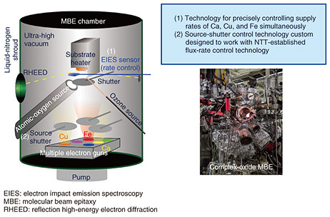
Fig. 1. Technology for growing high-quality complex-oxide superlattices.
An atomic-resolution scanning transmission electron microscope (STEM) equipped with an element-distinctive electron energy-loss spectroscopy (EELS) apparatus enabled direct observation of the atomic arrangements in the superlattices and evaluation of their crystallinity. The capability of visualizing atomic arrangements has been of great help in optimizing the growth conditions for such superlattices composed of materials with different crystal structures.
Our newly discovered and synthesized artificial-superlattice high-Tc superconductor [(CaCuO2)n/(Ca2Fe2O5)m]N has a Tc below −223°C, which does not reach the highest record for cuprates; nevertheless, we have demonstrated that a new superconductor can be synthesized by stacking two layers with completely different crystal structures. This suggests that the creation of artificial superlattices with even higher Tc by changing the material combined with IL-CaCuO2 is possible. It had not been clear why the IL-CaCuO2 layer, which is responsible for superconductivity in the superlattice, does not exhibit superconductivity by itself; however, through our research, we were able to clarify the mechanism by which the IL-CaCuO2 layer exhibits superconductivity when embedded in the superlattice. As shown on the left side of Fig. 2, in bare IL-CaCuO2 layers, the CuO2 planes, the playground of superconductivity are discontinuous due to the displacement of the atomic arrangement. In contrast, as shown on the right side of Fig. 2, when embedded in the superlattice, the pristine CuO2 planes are formed.
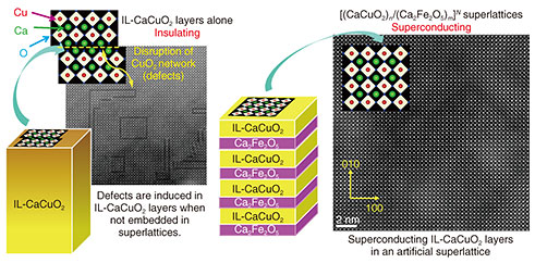
Fig. 2. The reason why IL-CaCuO2 layers exhibit superconductivity when embedded in the superlattice structure.
Drs. Ai Ikeda and Yoshiharu Krockenberger have been the main players in achieving these research accomplishments, which have been published in four scientific papers [1–4], leading to an invited talk in an international conference in 2021. We will be giving two more invited talks in November and December 2023. Dr. Ikeda received the 50th (Spring 2021) Japan Society of Applied Physics (JSAP) Young Scientist Presentation Award and the 14th JSAP Superconductors Division Young Scientist Award for an Excellent Article (March 2023), proving our research has been highly evaluated. Going forward, aiming for a higher Tc superconductor, we will try to establish material-design guidelines by varying the number of IL-CaCuO2 layers in one superlattice cell as well as using empirical rules concerning the types of charge-reservoir layers in materials that exhibit high Tc.
Through such activities, we intend to elucidate the mechanism of high-Tc superconductivity in cuprates. As represented by the study of infinite-layer materials such as IL-CaCuO2, we have reported that the electronic phase diagram, which is the key to comprehending the mechanism of superconductivity in cuprate superconductors, is strongly affected by the integrity of the CuO2 planes, the playground of superconductivity [5]. Although it is on cuprates that slightly differ from those we have been studying, another research group has recently reported similar results [6], which is of great interest from the viewpoint of comprehending the mechanism of superconductivity.
—Thin-film growth technology is important in terms of creating new materials and elucidating phenomena associated with them, right?
New substances and materials are generally synthesized either by reactions in beakers or flasks or, in the case of oxides, by solid-state reactions in which powders of constituent materials are mixed and fired in a furnace to synthesize bulk materials. In contrast, NTT aims to create new materials through thin-film synthesis—in which atomic beams of constituent elements are supplied and reacted under ultra-high vacuum—using the world’s most-advanced multi-source oxide molecular beam epitaxy (MBE) with high-precision control of evaporation rates that we have developed and improved over the years. The following are three key technologies: (i) for evaporating high-melting-point elements (≥ 2000°C) by high-energy-electron irradiation; (ii) for controlling the evaporation rates of multiple elements with high accuracy and in real time by using electron impact emission spectroscopy (EIES); and (iii) for oxidizing materials under ultra-high vacuum conditions by using ozone and atomic oxygen.
Our thin-film growth technology has been applied to synthesize new materials and prepare high-quality thin films of materials already in existence; however, to prepare the highest-quality thin films, it has been necessary to optimize the growth conditions through several hundreds to a thousand trial-and-error runs. To address this issue, we used process informatics to develop a methodology, algorithm, and program suitable for optimizing the thin-film growth conditions, which enabled us to efficiently prepare the world’s highest-quality thin films in less than 50 growth runs (Fig. 3). This is the second example of our major accomplishments mentioned at the beginning, i.e., (ii) the development of a pioneering and efficient method for growing high-quality thin films. In addition to establishing the superlattice-formation technology mentioned above, this technology has made rapid progress in the past five years or so thanks to the collaboration between NTT Basic Research Laboratories and NTT Communication Science Laboratories, where Dr. Yuki K. Wakabayashi has been playing a central role.
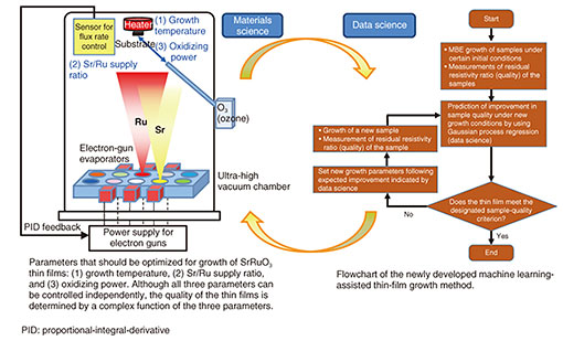
Fig. 3. Synergetic integration of materials science and data science.
The development of this method, called machine-learning-assisted molecular-beam epitaxy (ML-MBE), enabled us to demonstrate the magnetic Weyl semimetal state by using ultra-high-quality SrRuO3 thin films, our main accomplishment (iii) mentioned at the beginning. The compound SrRuO3 has been studied extensively from the viewpoints of both physics and applications because both metallic and ferromagnetic states are inherent in it, and it has a perovskite structure like many other complex oxides that have been widely studied in the field of oxide electronics. Since only limited sizes of single crystals of SrRuO3 were obtained until recently due to difficulty in crystal growth, research on physical properties has mainly been conducted using thin-film specimens. We used ML-MBE and successfully prepared the world’s highest-quality SrRuO3 thin film. This highest-quality thin film enabled us to demonstrate that SrRuO3 is a novel material in a unique quantum state: metallic, ferromagnetic, and Weyl semimetal states simultaneously occur in it [7−9]. These research outcomes have been published in many papers (approaching 15) first authored by Dr. Yuki K. Wakabayashi.
What is common sense in one field may not be in another, so a team of researchers with various backgrounds can turn something that does not seem common sense into something that is
—Please tell us what you keep in mind as a researcher.
We are currently researching as a team, but as a team manager, I try to take a bird’s-eye view when searching for research themes and subjects, and when interpreting experimental results. Regarding research themes, I first set a major theme and then leave the rest to our team members while making sure to respect their autonomy. Of course, I give advice based on my own experience and knowledge, and some problems can be solved based on that experience; however, a dilemma arises if we put too much emphasis on that experience: our ideas and research will become more and more predictable. I believe that this balance between past-experience-based advice and on-the-fly thinking by individual researchers must be kept in mind to maximize the strengths of a research team consisting of members of different generations. Regardless of generation, what is common sense in one field is often not in another. Fortunately, our team members have various expertise and backgrounds, and pursuing research while discussing among themselves often leads to unexpected ideas and results; thus, what was thought to be not common sense yesterday may become so tomorrow.
I also value the opportunity to talk face-to-face as we research as a team. I spend a lot of time on management-related desk work and in meetings, and it is sometimes difficult to find time to talk directly with the team members, but the limited time I can find conversely highlights the importance of such opportunity. Under the restrictions on laboratory attendance during the COVID-19 pandemic, I prioritized, as much as possible, attendance of the team members involved in experiments and I myself shifted to teleworking. Now that the restrictions have been lifted, I feel that face-to-face discussions in the lab and other places deepen our mutual understanding of the research themes and results. I hope this shift back to face-to-face discussion will lead to new discoveries.
NTT Basic Research Laboratories has an external evaluation committee called the Advisory Board, whose members include prominent researchers, including Nobel Prize laureates. Thus far, we have held twelve Advisory Board Meetings once every two years. In those meetings, the members of the Advisory Board visit the Laboratories to hold discussions and give evaluations and recommendations on our research system, research plans, and progress of research, and related matters. In 2021, during the COVID-19 pandemic, we were forced to hold the meeting online, but one of the members commented on my presentation that “This research effort is unique in the world, and this presentation is now achieving incredible results.” Even though I was distressed because we could not proceed with experiments and research as we wanted and could not make direct discussions due to the pandemic, that comment encouraged me a lot.
—What do you aim to achieve as a researcher in the future?
The discovery of materials that exhibit superconductivity at ambient pressure and room temperature is the ultimate goal of researchers involved in superconductivity. Although there are many possible approaches to discovering and synthesizing such materials, I want to focus on using thin-film growth methods. Although further study and verification are needed to determine the specific composition and crystal structure to target, fortunately, recent advances in theoretical and computational science have made it possible to predict with a high degree of accuracy the stability and electronic structure of materials that have not yet been synthesized. It has also become possible to (i) estimate the phonon structures of yet-undiscovered hypothetical materials and the magnitude of electron-phonon interactions in those materials and (ii) predict the superconducting transition temperature to some extent. We plan to incorporate such an approach while exploiting joint research with other institutions.
Even if a new material is discovered, it usually takes a certain amount of time before it can be put to practical use. However, if a material that exhibits superconductivity at room temperature and ambient pressure were put to practical use, it would be possible to transmit and supply electric power using direct current in a lossless manner, and if that material were used for wiring in circuits, problematic heat generation would be greatly reduced, thereby contributing to resolving environmental and energy issues. As a researcher, I am grateful for being able to conduct research at a time when materials that exhibit superconductivity at temperatures close to room temperature—though under ultra-high pressure—have been discovered, and I want to challenge myself to achieve the ultimate goal, though it will not be achieved overnight.
Streamline your research process and take detours once in a while
—What is your message to younger researchers?
First of all, I want to thank all the team members who have achieved outstanding results one after another, despite the great headwind of the COVID-19 pandemic, and NTT Communication Science Laboratories and other collaborators for their sincere efforts. To next-generation researchers, including those who are not necessarily directly involved in our research, I want to say the following. It is important to improve time performance so that we can achieve results and success in a limited amount of time. It is natural that people tend to focus on this time keeping, but I also want to point out that it is also important to take a detour once in a while. In the aforementioned research on artificial superlattices that exhibit superconductivity, it may sound as if we had taken the shortest route, but, in fact, we took quite a few detours. As a result of those detours, we discovered the unexpected phenomenon, disruption of the superconducting layer due to defects, and we were able to proceed with our research with a deep understanding of the significance of superlattice formation in preventing such disruption. Although the improvement in efficiency of the process for optimizing growth conditions through process informatics may seem to contradict this story, that efficiency improvement has also given us room to take a detour in our research on SrRuO3.
I also recommend that if you get a chance, you should experience a stay abroad. Living abroad means, at least in the short term, your research at that point in time will be interrupted. I think that from the standpoints of work as well as family and personal life, the timing when “everything is in order now and I can stay abroad without any problems or worries” will almost never come around. Today, we can make contact with people from different countries at academic conferences and other gatherings through web-conferencing systems and other means. Even so, I think that the experience of living abroad is still very significant. One example of this significance is to experience firsthand cultural differences and differences in ways of thinking; however, I also feel that experiencing other aspects that cannot be adequately expressed in words is more significant. I went to Stanford University in the USA for eleven months from 2004 to 2005 as a joint researcher. The primary significance was the deep and fruitful discussions I had with local researchers, but that is not all. For example, I was able to form valuable contacts and then expand that network of contacts, which helped us to accept an internship student from the University of Twente in the Netherlands from October 2022 to May 2023. Going abroad may not necessarily lead directly to research results in the short term; in the long term, however, the presence or absence of such experience will make a difference in your range of thinking and approaches to research.
References
| [1] | Y. Krockenberger, A. Ikeda, K. Kumakura, and H. Yamamoto, “Infinite-layer Phase Formation in the Ca1-xSrxCuO2 System by Reactive Molecular Beam Epitaxy,” J. Appl. Phys., Vol. 124, 073905, 2018. https://doi.org/10.1063/1.4985588 |
|---|---|
| [2] | A. Ikeda, Y. Krockenberger, and H. Yamamoto, “Molecular Beam Epitaxy of Electron-doped Infinite-layer Ca1-xRxCuO2 Thin Films,” Phys. Rev. Mat., Vol. 3, 064803, 2019. https://doi.org/10.1103/PhysRevMaterials.3.064803 |
| [3] | Y. Krockenberger, A. Ikeda, and H. Yamamoto, “Atomic Stripe Formation in Infinite-layer Cuprates,” ACS Omega, Vol. 6, pp. 21884–21891, 2021. https://doi.org/10.1021/acsomega.1c01720 |
| [4] | A. Ikeda, Y. Krockenberger, Y. Taniyasu, and H. Yamamoto, “Designing Superlattices of Cuprates and Ferrites for Superconductivity,” ACS Appl. Electron. Mater., Vol. 4, pp. 2672–2681, 2022. https://doi.org/10.1021/acsaelm.2c00209 |
| [5] | H. Yamamoto, Y. Krockenberger, and M. Naito, “Epitaxial Growth of Superconducting Oxides,” Chapter 5 in Epitaxial Growth of Complex Metal Oxides (Eds.: G. Koster, M. Huijben, G. Rijnders), 2nd edition, Elsevier, pp. 95–127, 2022. |
| [6] | K. Kurokawa, S. Isono, Y. Kohama, S. Kunisada, S. Sakai, R. Sekine, M. Okubo, M. D. Watson, T. K. Kim, C. Cacho, S. Shin, T. Tohyama, K. Tokiwa, and T. Kondo, “Unveiling Phase Diagram of the Lightly Doped high-Tc Cuprate Superconductors with Disorder Removed,” Nat. Commun., Vol. 14, 4064, July 2023. https://doi.org/10.1038/s41467-023-39457-7 |
| [7] | K. Takiguchi, Y. K. Wakabayashi, H. Irie, Y. Krockenberger, T. Otsuka, H. Sawada, S. A. Nikolaev, H. Das, M. Tanaka, Y. Taniyasu, and H. Yamamoto, “Quantum Transport Evidence of Weyl fermions in an Epitaxial Ferromagnetic Oxide,” Nat. Commun., Vol. 11, 4969, 2020. https://doi.org/10.1038/s41467-020-18646-8 |
| [8] | Y. K. Wakabayashi, T. Otsuka, Y. Krockenberger, H. Sawada, Y. Taniyasu, and H. Yamamoto, “Machine-learning-assisted Thin-film Growth: Bayesian Optimization in Molecular Beam Epitaxy of SrRuO3 Thin Films,” APL Mater., Vol. 7, 101114, 2019. https://doi.org/10.1063/1.5123019 |
| [9] | Y. K. Wakabayashi, Y. Krockenberger, T. Otsuka, H. Sawada, Y. Taniyasu, and H. Yamamoto, “Intrinsic Physics in Magnetic Weyl Semimetal SrRuO3 Films Addressed by Machine-learning-assisted Molecular Beam Epitaxy,” Jpn. J. Appl. Phys., Vol. 62, SA0801, 2022. https://doi.org/10.35848/1347-4065/ac73d8 |
■Interviewee profile
Hideki Yamamoto received a B.S., M.S., and Ph.D. in chemistry from the University of Tokyo in 1990, 1992, and 1995. He joined NTT in 1995, and his principal research fields are thin-film growth, surface science, and condensed-matter physics. He was a visiting scholar at the Geballe Laboratory for Advanced Materials, Stanford University, USA (2004–2005). He is currently executive manager of Multidisciplinary Materials Design and Science Laboratory, NTT Basic Research Laboratories. He received the 2nd Young Scientist Presentation Award (1997) from the Japan Society of Applied Physics (JSAP) and the 20th Superconductivity Science and Technology Award (2016) from the Forum of Superconductivity Science and Technology, the Society of Non-traditional Technology. He is a member of JSAP, the Physical Society of Japan, the Japan Society of Vacuum and Surface Science, the American Physical Society, and the Materials Research Society.