|
|||||||||||
|
|
|||||||||||
|
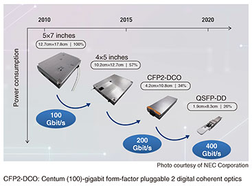
Feature Articles: Efforts toward the Early Deployment of IOWN Vol. 22, No. 1, pp. 73–79, Jan. 2024. https://doi.org/10.53829/ntr202401fa9 Photonics-electronics Convergence Devices Enabling IOWN—Development of Second- and Third-generation DevicesAbstractThis article presents second- and third-generation photonics-electronics convergence devices developed at NTT Device Innovation Center. The target applications and technical requirements for each generation of the devices are described. The advantages that can be obtained from photonics-electronics convergence devices and the technical points to achieve such advantages are also explained. Keywords: photonics-electronics conversion, silicon photonics, co-packaged optics  1. Second- and third-generation photonics-electronics convergence devicesSecond-generation photonics-electronics convergence devices are designed for use in digital coherent optical transceivers, which play an important role in optical communication network systems. By using a new optical technology called silicon photonics, we developed photonics-electronics convergence devices that make it possible to miniaturize optical transceivers and reduce their power consumption, and put them into practical use. In the first half of this article, the progress of digital coherent optical transceivers, advantages of silicon photonics, and features of photonics-electronics convergence devices we developed are described. Third-generation photonics-electronics convergence devices are intended to provide short-distance optical connections between racks and printed circuit boards (PCBs) in datacenters. With the increase in wide-bandwidth applications such as artificial intelligence, machine learning, augmented reality, and extended reality, network traffic in datacenters is increasing, and the accompanying increase in power consumption is a major challenge. In the second half of this article, our approach to address this challenge, which focuses on a new packaging technology called co-packaged optics (CPO), is described. 2. Miniaturization of optical transceivers and application of silicon photonicsDigital coherent optical transmission technology can compensate for signal degradation in optical transmission by using powerful compensation on the basis of digital signal processing and has been developed for transmission over long distances, namely, from several-hundred kilometers to several-thousand kilometers. Digital coherent optical transmission technology is also being applied to relatively short-distance (about 100 km) transmission, such as datacenter interconnects (DCIs), for which growth in traffic is particularly noticeable. The Optical Internetworking Forum (OIF) [1], an industry organization that develops technical standards for devices for optical transmission, stipulates requirements for power consumption and size of optical transceivers for digital coherent optical transmission. Every few years since 2012, OIF has published a new specification for digital coherent optical transceivers requiring a reduction in size. As shown in Fig. 1, such transceivers are becoming smaller, lower power consuming, and have faster transmission speed. The size of the transceiver has recently been reduced from 5 × 7 inches (12.7 × 17.8 cm) in 2012 to about 2 × 8 cm today (quad small form-factor pluggable double density (QSFP-DD) [2]), and over that period, its transmission speed has increased from 100 to 400 Gbit/s while its power consumption has decreased by about 75%.
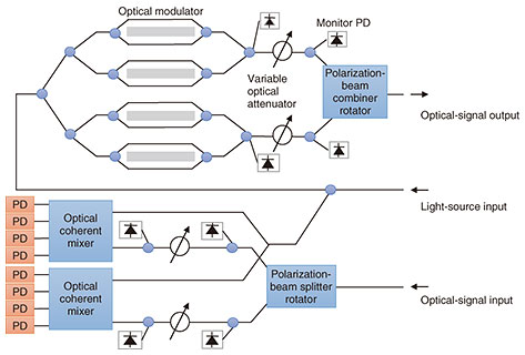
The need for smaller, lower power consumption, and higher-speed digital coherent optical transceivers is driven by the need for high-density installation of such transceivers in datacenters and other facilities. The demand for optical transceivers continues to grow annually, and the need for change to improve their cost performance and producibility is also growing. A digital coherent optical transceiver consists of a digital signal processor (DSP), analog electronic circuit (driver), which amplifies electrical signals, and optical modulator, which converts electrical signals into optical signals and outputs them, on the transmitter side; an optical receiver, which receives optical signals and converts them into electrical signals, and analog electronic circuit (trans-impedance amplifier (TIA)), which amplifies electrical signals, on the receiver side; and a laser-light source that serves as the local light source for transmitting and receiving. In conventional optical transceivers, optical devices such as optical modulators and receivers in the above-described configuration have been fabricated as individual packaged devices using optical material systems most suitable for their functions. For example, lithium niobate and indium phosphorus are used as materials for optical modulators. However, limitations on device size have made it impossible to miniaturize optical transceivers as required, so attention has turned to miniaturization and integration of optical devices through silicon photonics. We at NTT Device Innovation Center recognized the potential of silicon photonics early on and have continued researching and developing it. The advantages of silicon photonics have long been considered its contribution to device miniaturization and high productivity based on the mature semiconductor fabrication process. However, it is difficult to implement a light-source function with silicon photonics, and functions such as optical wavelength filters (which require precise control of the phase of light) are not suited to silicon photonics. Its characteristics also depend on the polarization of light (i.e., high polarization dependence). However, silicon photonics is a good match for digital coherent technology. The circuit configuration of the optical device of a digital coherent optical transceiver is shown in Fig. 2. The optical modulator consists of four modulation circuits and a polarization-beam combiner rotator, while the optical-receiver circuit consists of a polarization-beam splitter rotator, two optical coherent mixers, and eight photo detectors (PDs). Monitor PDs for monitoring optical-signal power for transmission and reception, and variable optical attenuators are also needed. These circuits do not require precise control of the optical phase, and their polarization dependence is not a problem because the polarization is processed separately. Silicon photonics, which has a large polarization dependence, is also suitable for circuits that control polarization such as a polarization-beam combiner rotator (splitter rotator). In conventional material systems, different optical components are integrated in the package to fabricate a polarization controller; in contrast, silicon photonics has the advantage in that different optical components can be integrated on a single chip. The integration of a large number of PDs with silicon photonics is also relatively easy.
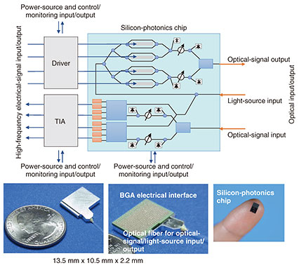
Taking advantage of the above-described features of silicon photonics, we developed a silicon-photonics chip for optical transceivers by integrating all optical circuits other than the light source. All the components shown in Fig. 2 are integrated on a single silicon-photonics chip. 3. Second-generation photonics-electronics convergence device: coherent optical subassemblySecond-generation photonics-electronics convergence devices use silicon photonics and are intended for application to small optical transceivers. We developed a coherent optical subassembly (COSA) [3] and put it into practical use as a second-generation photonics-electronics convergence device. The configuration and external appearance of our COSA are shown in Fig. 3. In addition to a silicon-photonics chip that integrates optical circuits, a driver that drives the optical modulator, and TIA that converts the output current of the receiving PD into a voltage signal and amplifies it are mounted in a single package. The development of our COSA has made it possible to fabricate a simple and compact optical transceiver with only three key devices: a DSP, COSA, and laser source.
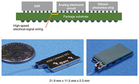
Our COSA was initially intended for use in DCIs between distributed datacenters, which at the time were beginning to attract attention as an application for digital coherent communications. The standardization of optical transceivers for DCIs was promoted as a transmission distance of 80 to 120 km, transmission speed of 400 Gbit/s, and QSFP-DD as the form factor (approx. 2 × 8 cm), which is considerably smaller than conventional transceivers. We developed our COSA as a second-generation photonics-electronics convergence device for embodying such a compact optical transceiver. As shown in Fig. 3, the size of the mounted silicon-photonics chip is approximately 4 × 6 mm, and the size of the package of our COSA is 13.5 × 10.5 × 2.2 mm, which makes it small enough to be mounted inside a transceiver with the QSPF-DD form factor. The factors that make it possible to downsize our COSA from the conventional package of optical devices include the omission of the temperature-control unit and the fact that the package of our COSA does not need to be hermetically sealed. These factors are the result of achieving temperature-independent characteristics and moisture resistance by applying a unique optical-circuit design while taking full advantage of the material stability of silicon. The non-hermetic packaging also enables a simple configuration in which the end face of the optical fiber is directly connected to the silicon-photonics chip, contributing to miniaturization and high productivity. In addition to the above advantages, our COSA offers excellent ease of use and producibility when mounted on a PCB of an optical transceiver. Our COSA uses (i) a ball grid array (BGA) as the electrical-signal interface and (ii) optical fiber as the optical-signal interface as with conventional packages, but the optical fiber is directly bonded to the silicon-photonics chip and is configured with materials that can withstand reflow soldering temperature (approximately 250°C). Most conventional optical devices require individual mounting processes after mounting other electronic components on the package substrate by solder printing and reflow. In contrast, thanks to its BGA interface and improved heat resistance, the components of our COSA can be mounted by solder printing and reflow automatically and simultaneously with other electronic components. This fabrication process of our COSA represents a revolutionary change in optical or photonics-electronics convergence devices. Our COSA can be mounted on an automated assembly line like other electronic devices in a manner that greatly simplifies and streamlines the assembly process of an optical transceiver. It became commercially available in 2020 and is currently being used in many compact digital coherent optical transceivers. 4. Second-generation photonics-electronics convergence device: coherent co-packageDuring the development of the second-generation photonics-electronics convergence devices that will follow our COSA, we have been promoting further integration of devices. Our COSA is a photonics-electronics convergence device that integrates a silicon-photonics chip, i.e., optical circuits, a driver, and TIA, i.e., analog electronic circuits, in a single package. We have further advanced this photonics-electronics conversion technology by mounting a DSP and a COSA in a single package (coherent co-package). The configuration and appearance of a coherent co-package are shown in Fig. 4. In addition to a silicon-photonics chip and an analog electronic circuit supporting a transmission speed of 400 Gbit/s, the same as that of our COSA, a DSP is also mounted on a single package substrate, which results in a package size of 21.9 × 11.5 × 2.3 mm. It is small enough to be mounted inside a QSPF-DD-form-factor transceiver with room to spare. Like our COSA, it uses a BGA interface, and components can be mounted through the automated solder printing and reflow.
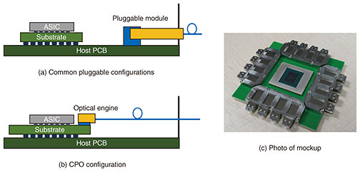
Since signal speeds are continually increasing, the performance of the high-speed electrical-signal wiring connecting the DSP and a COSA is particularly important. The aim with the coherent co-package is therefore to maximize the performance of the wiring by incorporating it into the package substrate and reducing its length, as shown in Fig. 4. This eliminates the need to design high-speed wiring to connect the DSP and a COSA in an optical transceiver, so the development period for the optical transceiver can be shortened. Having become commercially available in 2023, coherent co-packages providing a transmission speed of 400 Gbit/s are expected to be used in compact digital coherent optical transceivers. 5. Third-generation photonics-electronics convergence devicesIn a datacenter, which must handle large amounts of traffic, a large number of server racks are connected in a two- or three-tier tree-like configuration using switches. Graphics-processing-unit clusters are often set up to execute dedicated processing for artificial intelligence and machine-learning applications, and large-scale clusters are connected via switches. Many optical transmission devices, including high-capacity switches, have an array of pluggable optical transceivers on the front panel. As shown in Fig. 5(a), the application specific integrated circuit (ASIC) and pluggable transceiver in the body of the switch are connected by electrical wiring on the host PCB. As signal speed increase, transmission loss on the host PCB increases rapidly, so advanced signal-compensation circuitry for accurate signal transmission is required, and power consumption is thereby increased. The power consumption of large-capacity switch ASICs is more than 500 W, 30% of which is accounted for by input/output circuits for high-speed electrical-signal-wiring transmission. To reduce this power consumption, it is effective to place the optical transceiver as close to the switch ASIC as possible, and a new packaging approach called near package optics (NPO) or co-packaged optics (CPO) is attracting attention for that purpose (Fig. 5(b)). Although the transceiver cannot be plugged into or unplugged from the front-panel side, it is expected to reduce the total power consumption of the switch and accommodate more optical fibers at the front panel. Distinguished from conventional front-panel pluggable transceivers, optical transceivers used in NPO or CPO are called optical engines. A mockup of the prototype optical engine we are developing, mounted around the switch ASIC, is shown in Fig. 5(c). On the basis of the specifications established by OIF, the optical engine measures about 50 × 20 × 7 mm and has a transmission speed of 3.2 Tbit/s. Silicon photonics, which has begun to be used in second-generation photonics-electronics convergence devices, is used in the optical engine; however, the main difference is that the optical circuits for PAM4 (4-level pulse amplitude modulation) transmission are integrated in multiple channels instead of coherent circuits.
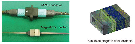
The optical engine accommodates up to just under 70 single-mode optical fibers. For a 51.2-Tbit/s switch using 16 3.2-Tbit/s optical engines for input and output, approximately 1000 optical fibers are accommodated in the switch. Since the fiber routing for this configuration is complicated, the optical engine should have an optical connector interface so that the optical engine and optical fiber can be mounted separately. Multi-fiber push-on (MPO) connectors are commonly used as multi-fiber optical connectors; however, 70 optical fibers cannot be accommodated in the 20-mm width of a single connector. Thus, we are developing our own multi-fiber compact connectors [4]. These in-house connectors use the attractive force of the magnet as a pressing force between the plug and receptacle, so springs and housing parts, which are indispensable components of MPO connectors, can be omitted, and the connector can thereby be significantly miniaturized. As shown in Fig. 6, we constructed a prototype of this magnetic connector to verify the principle of this connector and confirmed that its size (volume ratio) is one-tenth that of a conventional MPO connector. The image on the right of Fig. 6 visualizes the magnetic field around the prototype and shows that the magnetic force is efficiently confined.
6. Future developmentsWe are developing second-generation photonics-electronics convergence devices to achieve even higher transmission speeds. OIF is currently discussing the next generation of coherent optical transceivers with transmission speeds of 800 Gbit/s. We have also started developing a silicon-photonics chip for supporting this higher-speed transceiver and we developed a prototype chip [5]. As the next step, we are currently researching the technology for a coherent co-package that can support a transmission speed of 800 Gbit/s. For the development of third-generation photonics-electronics convergence devices, we will not only develop silicon photonics and optical connectors but also create an ecosystem to promote the transition to CPO. References
|
|||||||||||