|
|||||
|
|
|||||
       |
Rising Researchers Vol. 22, No. 3, pp. 12–16, Mar. 2024. https://doi.org/10.53829/ntr202403ri1  High-performance Optical Devices with Integration of Heterogeneous Materials Accelerating the Future of Photonics-electronics Convergence TechnologiesAbstractThe transmission capacity of electrical wiring has come to be viewed as a bottleneck in system processing performance in conjunction with increases in datacenter traffic and the development of high-performance large-scale integration (LSI) by transistor miniaturization. To solve this problem, there is a strong demand for photonics-electronics convergence technologies for applying optical transmission that can easily increase capacity to wiring positioned close to electronic circuits. In this article, we talk with NTT Distinguished Researcher Tatsurou Hiraki to learn about his research and development of “high-performance optical devices with integration of heterogeneous materials” as a rising researcher opening up a new future. Keywords: photonics-electronics convergence, integration of heterogeneous materials, optical device
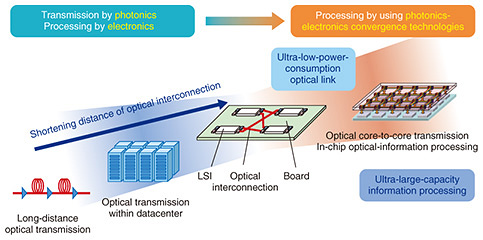
Achieving high-performance optical devices using the best features of different materials—Dr. Hiraki, please explain “high-performance optical devices with integration of heterogeneous materials” that you are currently researching. In high-performance optical devices with integration of heterogeneous materials, I am researching and developing means of drawing out high performance by combining two or more materials in an optimal arrangement in contrast to past optical devices fabricated with a single-material system. As background to this research, I can point out dramatic increases in datacenter traffic and ongoing improvements in large-scale integration (LSI) performance. Because of these developments, transmission capacity of electrical wiring is becoming a bottleneck in system processing performance, and as a result, increasing the capacity and reducing the power consumption of optical wiring at datacenters and in computers is becoming increasingly important (Fig. 1).
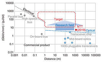
Immediately after entering NTT, I took up the research and development of devices for optical communication using silicon. At that time, however, I had to face the fact that these devices were inherently limited in performance due to the material properties of silicon, something that I was not pleased about. Then, after several years had passed and worrying every day about what I should research, a reorganization of NTT laboratories combined the group I was in with a department working on the integration of compound semiconductor lasers on silicon substrates. At first, I was a bit confused about the change in research themes, but thinking that “well, we are all one group now,” I actively took up the study of compound semiconductor technology that I had not been very familiar with up to then. As a result, since there were many things that I had so far given up on due to the material limitations of silicon, I came to think that maybe I could solve some of those problems by using compound semiconductor materials. But then, focusing on the fact that both silicon and compound semiconductors have advantages and disadvantages, I also came to wonder whether an optical device structure that combines only the best parts of both types of materials could be used to fabricate various types of optical devices superior to those of the past without being limited to lasers. This research that I began in this way is now my current research theme that aims to achieve high-performance optical devices that combine two or more materials. —What are the issues surrounding conventional optical devices using only a single material? In the past, optical devices were fabricated separately using silicon, compound semiconductor material, or amorphous material, for example. Each type of material has its advantages and disadvantages. For example, indium phosphide (InP)-based compound semiconductors widely used in the fabrication of lasers feature excellent emission efficiency. Additionally, the advantage of a diode structure having n-type (negatively charged) and p-type (positively charged) regions is low electrical resistance, low optical loss, and high phase modulation efficiency in the n-type region. The disadvantage here, though, is that optical loss in the p-type region is extremely large. As a result, p-type semiconductors have become a limiting factor in the structure and performance of lasers and optical modulators. Silicon, however, which is widely used in the fabrication of electronic circuits, features optical loss in p-type regions less than that of InP-based materials and has properties conducive to low-cost, mass production. The emission efficiency of silicon, however, is extremely low, and it is inferior to InP-based materials in terms of electrical resistance, optical loss, and phase modulation efficiency in the n-type region, so those weak points of silicon material can limit the performance of optical devices and target applications. Additionally, while many types of materials exist for configuring optical devices, it is extremely difficult to find a material system that can satisfy all requirements by itself, so performance limitations governed by the properties of each type of material have been a major hurdle. Moreover, given that each material has its strong points and weak points, the general approach today in the field of optical devices is to first fabricate each optical component with optimal materials and to then mount each in a single module. In this type of process, however, integration density is limited by the size of each component, mounting precision, etc. It is therefore very difficult to use this conventional technique in achieving photonics-electronics convergence that aims to achieve high-density integration of optical transceivers at positions near electronic circuits (Fig. 2).
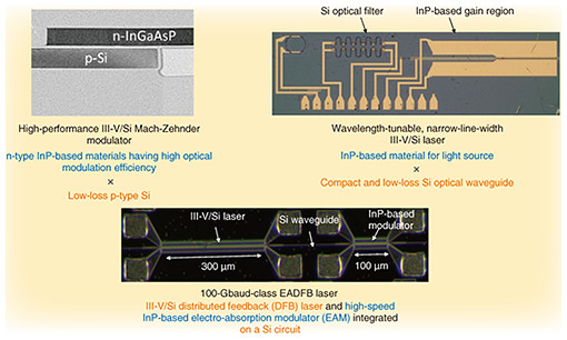
With these problems in mind, I have undertaken the integration of heterogeneous materials—mainly compound semiconductors and silicon—with the aim of achieving both high performance and high integration in optical devices like optical modulators and semiconductor lasers by combining the strengths of both types of materials. —Please tell us about some of the achievements you have already made in this research. For example, a silicon Mach-Zehnder modulator fabricated by conventional silicon-photonics technology suffered from performance limitations due to a tradeoff between modulation efficiency and optical loss. In my research, I overcame this performance limitation by combining low-loss p-type silicon and high-efficiency n-type InP-based material and achieved approximately four times or greater modulation efficiency (0.09 Vcm) with low optical loss compared with conventional technology. Additionally, by fabricating a laser that combines a membrane InP-based laser structure and a compact and low-loss Si optical waveguide, I reduced the optical loss caused by p-type InP-based material and achieved a compact wavelength-tunable laser. Recently, moreover, by developing an electro-absorption modulator (EAM) that can be integrated together with such a membrane laser on a low-loss Si waveguide, I succeeded in integrating an O-band EAM and optical source, which had been difficult to achieve by silicon optical circuits, and demonstrated 100 Gbit/s high-speed modulation operation (Fig. 3). These research achievements combine the respective strong points of silicon and compound semiconductor materials thereby drawing out a level of performance beyond conventional levels. They can be viewed as examples of successfully achieving high-density integration using compact Si optical circuits.
Furthermore, to integrate a high-performance wavelength filter with such a laser or optical modulator, I am working on technology for fabricating a silicon-nitride (SiN) waveguide having optical propagation loss about one order of magnitude smaller than that of conventional optical waveguides using silicon. This technology opens up the possibility of fabricating low-loss waveguides in a low-temperature process that inflicts no thermal damage on compound semiconductors. —What hardships have you had to face in your research? Looking at my research up to now, perhaps there are some people who would think, “It makes sense that combining materials with different features would improve performance.” It certainly would be great if combining materials could immediately improve performance, but in actuality, attempting to do so often ends in failure. The true difficulty lies in “fabrication technology” that aims to achieve integration without losing the good features of each of the materials being used. For example, the technology required for fine processing differs between the two types of materials of silicon and compound semiconductors, and how to fabricate a device without negatively affecting the material properties of both is a major research issue. Even if the performance that can be drawn out by combining materials can be understood theoretically by calculations, there are many problems that must be faced at the fabrication stage, and if working with new materials or structures, there is nothing but failure at first. The research of such fabrication technology is a trial-and-error process from one day to the next, and most of that research period is kept private and hardly talked about in research papers or elsewhere. Indeed, it may take several years until a paper can be presented, and in this sense, research can be mentally challenging. Believing in your research with all your heart is important to prevent yourself from becoming totally depressed during research, but it is also true that sometimes the direction of your research must be changed along the way. In actuality, there are many fatal problems that come to light when starting a fabrication project, and it may be necessary to remain calm and decide “staying on this course any longer is not going to work!” It is important that you do not cling to any one matter and that you retreat as needed. In addition, I believe that it is important within such a process of failing to actively search out the cause of failures and to increase the ratio of meaningful failures that can create a path to subsequent research. It is exactly an increase in meaningful failures that can be a major turning point in whether you eventually produce good research results. Aiming for core technologies in photonics-electronics convergence while exploring new research for the future without clinging to the past—Dr. Hiraki, what is your research vision going forward? At NTT, I belong to three research laboratories: NTT Nanophotonics Center within NTT Basic Research Laboratories, NTT Device Technology Laboratories, and NTT Device Innovation Center. NTT Basic Research Laboratories is engaged in basic research covering a wide range of fields from theoretical research to device fabrication technology. Here, you get the impression that each of its researchers is academically taking on the challenge of new things. NTT Device Technology Laboratories is engaged in research that pursues academic novelty while also being conscious of social needs with a view to practical application in the future. While themes that reflect the mission of the organization advance steadily among all the research groups here, individual researchers also adopt original approaches. Finally, NTT Device Innovation Center is the organization that, among all the organizations that I belong to, is the most practical in its orientation. It is involved in the commercialization of devices while working in cooperation with NTT Group companies and other companies that actually produce the devices. In this way, I am involved in research and development spanning a wide range of phases. This kind of environment where a researcher can undertake a wide variety of technical fields all at once from communication infrastructures to basic research is truly a great strength of NTT laboratories. In addition, it is an especially beneficial environment where I myself as a researcher can grow. Although I knew practically nothing about optical communications and optical devices before entering the company, I was able to start learning from the very beginning thanks to the gracious support I received from many top-class experts residing at NTT. There were also many times when I noticed the good points and bad points of my own technology through the discussions I had with researchers in other fields, so being able to come up with fresh ideas at any time in this way is likewise a great strength of NTT. When taking up a new challenge, I am fortunate in having opportunities to receive the cooperation of experts having technology that I lack, which gives me many chances to produce research achievements having a speedy impact or to establish new technology that might give rise to a paradigm shift. Among the readers of this article, there might be many whose current field of specialization differs from the research themes at NTT laboratories, but I think that viewpoints from other fields have the potential of making great changes to existing research. To any readers who are looking for an opportunity to change fields and pursue new research, I would say, “Let’s work together in accelerating the coming of a new future in optical communications.”
Reference
■Interviewee profileTatsurou Hiraki received his M.E. degree from Tohoku University in 2011 and entered NTT in the same year. He is a member of NTT Device Technology Laboratories, NTT Device Innovation Center, and NTT Nanophotonics Center within NTT Basic Research Laboratories. He received his Ph.D. degree in engineering from Tohoku University in 2017. Since 2022, he has been a Distinguished Researcher at NTT Device Technology Laboratories. He is engaged in the research and development of photonic integrated circuit technologies using silicon, compound semiconductors, and amorphous-material optical waveguides and optical devices for communications applying those technologies. |
||||