|
|||
|
|
|||
       |
Feature Articles: Technical Seminars at NTT R&D FORUM 2024 - IOWN INTEGRAL Vol. 23, No. 4, pp. 28–36, Apr. 2025. https://doi.org/10.53829/ntr202504fa2 The Future of Photonics-electronics Convergence Technology and Supercomputers
AbstractThis article presents a discussion on the forefront of photonics-electronics convergence technology, which is based on a technical seminar conducted at the “NTT R&D FORUM 2024 - IOWN INTEGRAL” held from November 25th to 29th, 2024. Keywords: photonics-electronics convergence, optical interconnect, supercomputer
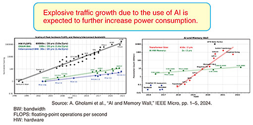
1. Presentation 1Membrane III-V photonic devices for in-package optical interconnectsMatsuo: One of the goals of NTT’s research on optical devices is reducing power consumption. The use of information and communication technology (ICT) equipment is rapidly increasing worldwide, and with the spread of cloud services and artificial intelligence (AI), datacenters are becoming larger. One large-scale datacenter requires as much electricity as generated by one nuclear power plant, and datacenters account for 2% of global electricity consumption. In Japan, concentrated in the Tokyo metropolitan area, datacenters account for 12% of Japan’s electricity consumption. NTT uses—mainly for communications and computers—0.7 to 1% of total electricity demand in Japan, so research and development on reducing power consumption is an urgent task for us. Since my specialty is optical technology, I will briefly review the history of optical technology. Information can be transmitted with two methods: wireless (e.g., mobile phones) and wired. The wired method is classified into two types: electrical interconnects, which send electrical signals carrying information through copper wire, and optical interconnects, which send optical signals carrying information through optical fiber. Electrical interconnects are slower in terms of transmission speed but more cost-effective when transmission distance is short. In contrast, optical interconnects are faster, so they are preferable when transmission distance is long. Optical fiber began to be used in inter-prefectural networks about 40 years ago in Japan, and is now widely used in longer networks such as submarine cable networks. As the processing power of ICT equipment has increased and transmission speeds have increased, it is now becoming more cost-effective to use optical interconnects even over shorter distances, such as in datacenters and supercomputers. In supercomputers, optical interconnects are almost always used for signal link, the distance of which is averaging about 20 m. In light of these circumstances, focusing on optical interconnects inside a package containing a photonics-electronics convergence device, I’ll explain why optical technology is applied not only to communications but also to computing. As the use of AI increases, traffic (i.e., communication volume) is expected to increase, and power consumption will continue to increase accordingly. In the left graph in Fig. 1, the black line represents the increase in computer performance, green line represents the increase in memory capacity, and blue line represents the increase in communication speed. The difference between the slopes of the black and green line is called the “memory gap,” and this memory gap is only getting wider as time progresses. This trend was driven by the use of AI, as shown in the graph on the right in Fig. 1. The number of parameters of Transformer models, shown as the red line, is increasing at an even faster rate than computer performance. Therefore, the amount of electricity required for communications is increasing.
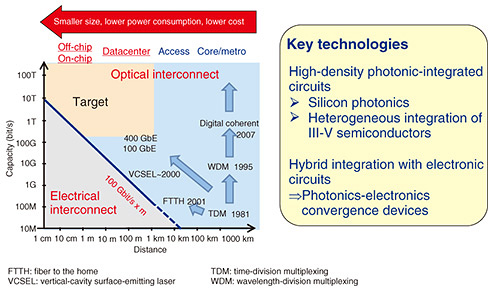
The target of our research and development is to introduce optical interconnects in shorter-distance transmissions where power consumption is high with electrical interconnects (Fig. 2). During this research and development, it is important to consider that devices must be small due to space constrains, and their power consumption and cost must be low. Photonic-integrated circuits satisfy these three requirements. We use silicon photonics, which uses the silicon complementary metal-oxide semiconductor (CMOS) process to fabricate photonic and electronic integrated circuits on silicon. Since compound semiconductors—rather than silicon—are used as materials of transmitters/receivers for the laser light required for optical communications, a technology for the heterogeneous integration is needed. Photonic-integrated circuits fabricated in this manner are then integrated in three dimensions with electronic circuits, creating a photonics-electronics convergence device.
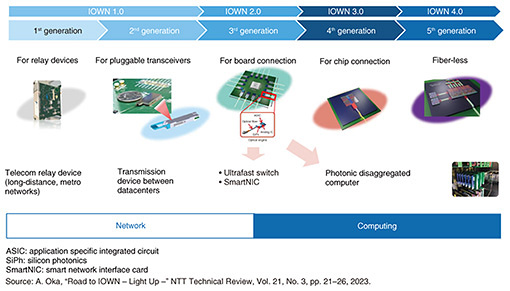
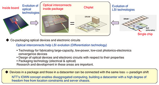
The roadmap for photonics-electronics convergence devices in regard to the Innovative Optical and Wireless Network (IOWN) is shown in Fig. 3. We aim to introduce optical interconnects between datacenters then between boards, between chips, and finally inside chips. Another point concerning this roadmap is that the distinction between communications and computing functions of a single chip will disappear. Therefore, if light is to be introduced to replace electricity for communications over the extremely short distances inside a chip, NTT, which has until now specialized in communications, will need to take on computing as well.
The time frame for developing photonics-electronics convergence devices has been set very short, which is challenging. One practical issue is that when laser light is emitted from large-scale integrated circuits (LSIs), a huge amount of energy is used in the electrical interconnect, and some of it is wasted. It is currently a global trend to eliminate such waste by physically placing optical devices, which consume less energy, closer to electronic circuits. However, compared with electronic devices, optical devices are fragile and difficult to replace, so how to create low-cost, durable, and reliable high-quality optical devices has become a research topic. Ensuring power is allocated to computing and effectively using computing resources without relying on physical locations of hardware through optical interconnectsMatsuo: Next, I’ll explain the need for opticalization of LSIs. The reason for the shift to optical technology is, naturally, related to power consumption. While the power consumption of a central processing unit (CPU) chip increases in a linear manner as its performance improves, the bandwidth used for off-chip communications increases exponentially. If this trend continues, the power available for the original purpose of computers—namely, computing—will decrease. To secure the power needed for computing, it is thus necessary to reduce power consumption through opticalization of LSIs. A typical LSI consists of a CPU, graphics processing unit (GPU), input/output (I/O), memory, etc. on a single chip. However, as chips became larger, and the associated problems with throughput in manufacturing became apparent, the chip began to be divided into multiple smaller chips called chiplets, which can be combined as needed. Therefore, performance improvement (bandwidth and power consumption) in communications between chiplets is also important. In-package optical interconnects that we aim for and the shift from chips to chiplets are heading in the same direction (Fig. 4). I believe that the introduction of optical interconnects in packages will enable the continued evolution of LSIs. Some companies in the United States are talking about implementing optical circuits on 300-mm wafers. Optical technology thus becomes more important as package size increases.
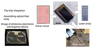
Transmission loss of light is roughly constant (about 0.2 dB), whether light is transmitted over a distance of 2 cm or 2 km. It is thus possible to achieve “disaggregated computing” in which different types of computing resources are connected using long-distance, broadband, low-power photonics-electronics convergence technology. As proposed by NTT, disaggregated computing enables the collecting of memory from various locations to achieve scalable computing and resolve memory shortages. Importance of photonics-electronics convergence devices that integrate compound semiconductors and siliconMatsuo: As I mentioned earlier, although it is possible to fabricate electronic circuits using silicon, it is not possible to fabricate laser light using silicon. The most-common method to fabricate laser light is to place a device emitting laser light on silicon; however, to pass light through a 0.5-μm-wide optical waveguide, which is equivalent to an optical fiber, it is necessary to align the light-emitting part of the device with the optical waveguide, which is costly. At this R&D Forum, we are demonstrating that it is possible to fabricate a laser device on silicon at the wafer level. By making the laser device thinner than conventional ones, many benefits, such as strong optical confinement to the active layer, have been generated. This led to the creation of a photonics-electronics convergence device that is highly compatible with silicon photonics. Our research and development has progressed to the point that a 16-channel laser array can be placed on silicon to output a 1.6-Tbit/s signal. By integrating the laser array and CMOS driver circuit in three dimensions through flip-chip bonding, the distance between photonic and electronic circuits can be shortened, and power consumption can be significantly reduced. To achieve low power consumption quickly and at low cost, rather than designing the photonic and electronic circuits separately, it is important to consider them as a whole, and I believe that converting them into a photonics-electronics convergence device will become key in the future (Fig. 5).
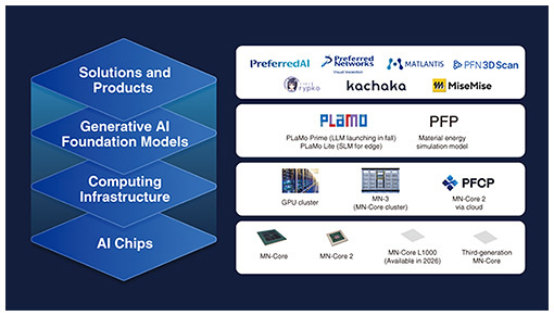
2. Presentation 2Towards sustainable AINishikawa: My name is Toru Nishikawa, and I’m chief executive officer of Preferred Networks, which has a business partnership with the NTT Group in the field of AI. Although we are not yet using photonics-electronics convergence technology, I believe that achieving optical interconnects with low power consumption at low cost will definitely become important in generative AI and foundation models, where on-chip and chip-to-chip interconnects play a crucial role in determining the performance of these models. Current AI, such as generative AI, is more compute-intensive in comparison with machine-learning AI; thus, the balance in the architecture is changing and the architecture itself is also changing. I’ll explain what kind of architecture we should aim for in the midst of these changes. At Preferred Networks, our business is vertically integrated with four layers: solutions and products, generative AI and foundation models, computing infrastructure, and the production of AI chips. There are many unknown aspects of the potential of generative AI and foundation models, and I believe that we are in a phase in which we need to research and develop various layers with agility to explore that potential, so we are conducting research and development on the four layers in a balanced manner (Fig. 6).
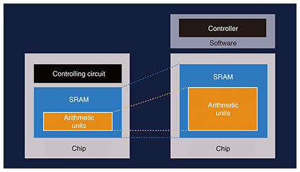
As Mr. Matsuo mentioned earlier, power consumption has become a huge problem today. The computing power required for cutting-edge AI systems is increasing exponentially, far exceeding that of the world’s-highest-performance supercomputers. While the potential of AI is higher, its power consumption and costs are also increasing, and it is a contradiction in that while the use of advanced AI can help reduce energy consumption, it uses a much larger amount of electricity than it can reduce. As an AI researcher, I must consider how to reduce this power consumption. As a solution to this problem, we developed a chip dedicated for AI called “MN-Core” from 2016 to 2019, and its second generation from 2020 to 2023. We developed AI chips because there was already a shortage of GPUs used for AI, and even if 100,000 GPUs were manufactured, it would still not be enough. Ensuring computing power and reducing power consumption are crucial for AI. To secure these crucial elements of AI, we began developing AI chips in-house. To reduce power consumption of MN-Core, a large portion of the transistor is used for the arithmetic unit and on-chip memory, called static random-access memory (SRAM), and the controlling circuit is kept to a minimum and the control is offloaded to software. As a result of this chip architecture, power consumption has been significantly reduced (Fig. 7).
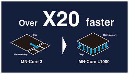
We are currently using MN-Core in-house and have found that the imbalance of workload between AI inference and AI training, such as the inference part is light and the training part is very heavy, has a significant impact on chip performance. We believe that by optimally designing the architecture of MN-Core, we can create a low-cost processor that consumes low power while maintaining adequate performance. We are currently working on the third and fourth generations of MN-Core, and the third generation is scheduled for commercial sale in 2026. We are also focusing on compiling (translating programming code into machine language) software for MN-Core, and by successfully fusing software and hardware technology during development, we are increasing the number of AI models compatible with MN-Core software. Our supercomputers equipped with MN-Core won first place in the Green500 list of world’s most energy-efficient supercomputers three times (June 2020, June 2021, and November 2021). MN-Core has a very unusual architecture, but I believe we were able to prove that it is a new architecture that combines ease of use and cost performance through the ingenious integration of software and hardware. In accordance with our roadmap, we will separately develop MN-Core for inference and training, the optimal architectures of which differ. By leveraging new technologies, such as advanced packaging, we aim to develop flexible and application-specific processors optimized for each. For example, inference involves almost no arithmetic operations and requires heavy use of memory and interconnects, so it necessitates a high-speed, low-power technology such as photonics-electronics convergence (Fig. 8). By combining such technologies, we will be able to create a better chip architecture in a manner that will contribute to the development of large language models (LLMs).
Large-scale computers, such as supercomputers, are made up of complex ecosystems, so I believe it is important to build an excellent ecosystem within Japan and continue to grow it by constantly incorporating new technologies. From now onward, technology to scale-up computers will become increasingly important. Of course, scaling computers for running LLMs is important, but the world of AI does not end with LLMs. That is, increasing the speed of computers will bring more possibilities, and to make them a reality, I believe it is necessary to integrate various ecosystems and technologies, including highly efficient AI chips, interconnects, and chiplets. 3. DiscussionThe process leading up to the creation of MN-CoreMatsuo: I was very impressed by the idea of removing unnecessary components and controlling them with software to give more space to computing as the power used for computing becomes ever more limited. As far as I know, Preferred Networks has developed search engines and AI. Could you tell me in more detail why you thought the development of MN-Core was important? Nishikawa: In 2016, it was very difficult to obtain GPUs in Japan, and although we managed to purchase 1024 GPUs, the negotiations leading up to their acquisition were very tough. At that time, some companies in Japan were researching, developing, and selling architecture of processors, but they had weakness in their software and could not replace GPUs, so I thought that if things continued as is, GPUs would eventually become unavailable. Moreover, we had a goal with deep learning of achieving our ideal workload (namely, the amount of processing load on a computer), so we decided to design our ideal architecture of a processor ourselves. I believe a big part of that decision was the fact that I was fascinated by the idea of creating hardware. During my university days, I studied in the lab of a professor specializing in hardware. At a time when a supercomputer cost 100 billion yen, he said, “We are going to build a supercomputer for two billion yen by developing low-power-consumption and low-cost processors,” which astonished me. Although we could not achieve the desired performance, we were able to achieve fairly good performance at that cost. Given that course of events, I felt that building supercomputers would be very interesting, so I entered this field and believe this decision led to the development of MN-Core. Matsuo: When building hardware, such as a supercomputer, design is very important. Preferred Networks has many software researchers, so how do you accelerate hardware research? What do you keep in mind when recruiting people and producing results as a company? Nishikawa: We currently have about 80 members developing hardware and are focusing on how we can thoroughly verify the hardware they develop. When writing test vectors (data for evaluating the design content) for hardware and test cases, we try out various scenarios and try to prevent problems caused by bugs as much as possible. If a bug does occur, we focus on workarounds for how to fix it and prevent problems from occurring. The future of supercomputers and AIMatsuo: Regarding the issue of memory shortage, you mentioned three-dimensional integration of memory and CPUs to increase communication efficiency, bandwidth, and speed. I mentioned NTT’s disaggregated computing, but can a supercomputer that uses the entire datacenter work for AI and similar applications? Nishikawa: I believe that as well as improving the performance of datacenters, we should use AI to design supercomputers. Supercomputers are extremely complex systems, and their complexity is expected to increase. To ensure that these increasingly complex supercomputers operate stably, they must be properly designed, but that task is extremely difficult for humans. However, it can be handled by AI, and I believe it will be important to establish a process that enables AI and humans to work together to design supercomputers. Matsuo: If AI is tasked with designing a supercomputer, it might generate an overwhelming amount of designs that will be difficult for humans to verify their appropriateness, and it is possible that if we leave this verification to AI, it may determine something that is inappropriate to be appropriate. What can be done to address this issue? Nishikawa: I share those concerns. To address this issue concerning use of AI for verification, it is necessary to start by designing small circuits using AI and gradually build up expertise. I believe that computers will be able to design computers. To make this a reality, we must first separate tasks between what humans can and cannot do, and this separation process requires craftsmanship. Executing this process appropriately and discovering new design methods are key in creating new semiconductors. Many other issues, such as increasingly complex packaging hierarchy, increasing difficulty of dissipating heat, and integration of semiconductor layers, are difficult for humans to handle. By addressing these issues in designing semiconductors, I believe it is possible to deliver value that only Japan can provide. In other words, unless we address these issues, I think it will be difficult to find a winning scenario for manufacturing semiconductors in Japan. Matsuo: Regarding disaggregated computing, our current challenge is that the architecture required for a compact LLM and large LLM depend on how the boards are connected. Without an architecture that can be used flexibly, I don’t think future supercomputers will be able to run efficiently. Therefore, I’d like to ask you how MN-Core is made. Does one unit execute all calculations or are multiple units connected together to execute calculations? Nishikawa: MN-Core version 1 connects four dies in one package, version 2 consists of one die, and version 3 (under development) increases the integration density. It is important to separately design MN-Core for inference and training and develop a processor that can efficiently work and that is small, which makes it possible to reduce the amount of computation needed for efficient inference to about one-tenth or one-twentieth the conventional amount. In addition to reducing power consumption, addressing heat dissipation is also important, so we are conducting research and development while conducting simulations to investigate the balance between heat dissipation and power consumption. 4. Message to the audienceAiming for a world in which energy conservation is possible with AIMatsuo: Hardware research is often hit or miss, so we are conducting research through trial and error, and it is very difficult to work hard toward a goal with uncertainty. We are working hard with our partner companies to make such research useful to society. Since NTT laboratories are corporate research institutes but have a public responsibility, we need to think about the planet and society as a whole. As for the issue of energy consumption, to put it in extreme terms, if we don’t use the Internet, we can reduce energy consumption and will be friendly to the Earth; that is unrealistic, however. I think that AI can achieve a breakthrough on this issue. The energy consumption of AI is currently problematic, but I believe it is important to use the technology of NTT and Preferred Networks to aim for a world in which energy can be saved by using AI. I also believe that AI can be used in areas other than design devices. For example, AI can be used in factory-line management, that is, AI can monitor a production line, issue alarms, and make corrections if something goes wrong in a manner that creates a sustainable factory and leads to reduced power consumption. I think that the possibilities of AI will expand in such ways. Nishikawa: I think that the combination of hardware and software, and the balance between them, will become increasingly important in regard to supercomputers. I am often asked, “What does your company do?”, and I answer that our goal is to bring about innovation by fusing hardware and software in a well-balanced manner. To do that, we need to research both. AI-driven automation may eventually slow down, but I think in the world of entertainment and new devices, low-power edge devices using new materials, will continue to emerge. While it seems that there are almost no companies in Japan that enrich people’s lives from hybrid (private and public entities) perspectives, I am extremely impressed with NTT’s efforts in that regard. |
||