|
|||||||||||||||||||||||||||||||||||
|
|
|||||||||||||||||||||||||||||||||||
       |
Regular Articles Vol. 23, No. 10, pp. 83–91, Oct. 2025. https://doi.org/10.53829/ntr202510ra1 Micro-transfer Printing of III-V Membrane Photonic Devices on Various PlatformsAbstractWe demonstrate micro-transfer printing of III-V membrane lasers onto silicon photonics and thin-film lithium niobate (TFLN) platforms. The III-V membrane lasers feature high modulation efficiency and simple adiabatic tapers for efficient optical coupling. On silicon, direct modulation at 40 Gbit/s is achieved with low bias current. Integration with TFLN Mach-Zehnder modulators enables data transmission up to 128 Gbit/s. These results highlight the versatility and effectiveness of micro-transfer printing for heterogeneous photonic integration, and its potential for efficient use of III-V materials across a wide range of photonic platforms. Keywords: micro-transfer printing, silicon photonics, membrane lasers
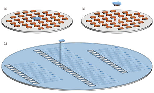
1. IntroductionSilicon photonics has emerged as a leading platform for large-scale photonic integrated circuits, driven by continuous advancements in semiconductor foundry technologies. A wide range of functions can be achieved in silicon photonics, including optical modulators based on the carrier-plasma effect, photodetectors integrated with germanium, and filters using silicon or silicon-nitride passive waveguides. However, efficient light emission from silicon remains a challenge due to its indirect bandgap nature. To overcome this limitation and enable the integration of lasers, light-emitting diodes, and semiconductor optical amplifiers, the incorporation of III-V materials onto silicon photonics platforms is essential. Several approaches have been explored for integrating III-V materials with silicon photonics, such as direct epitaxy on silicon-on-insulator (SOI) wafers, wafer-to-wafer and die-to-wafer bonding, and micro-transfer printing [1]. In this article, we focus on micro-transfer printing, as it enables expanded applications by facilitating the integration of various non-native materials—including III-V compounds, lithium niobate (LN) [2], cerium substituted yttrium iron garnet (Ce:YIG) [3], and even III-nitrides on flexible substrates [4]. Figure 1 illustrates the concept of micro-transfer printing. III-V-based devices are fabricated on their native III-V substrates as thin films with sacrificial layers. After forming tethers, the sacrificial layers are selectively etched, leaving the devices supported only by the tethers as coupons (Fig. 1(a)). An elastomer stamp then picks up the coupons by breaking the tethers (Fig. 1(b)) and positions them above the target silicon photonics wafers (Fig. 1(c)). The upper cladding of the target wafer is locally removed at regions designated for III-V integration. Finally, the coupons are attached to the silicon photonics wafer, and the elastomer stamp is carefully peeled away, leaving the coupons in place (Fig. 1(c)).
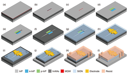
Micro-transfer printing enables the independent fabrication of both silicon and III-V devices using established fabrication lines. Additionally, in complex photonics integrated circuits such as wavelength-division-multiplexed transceivers, the area required for III-V materials is typically much smaller than the total circuit area. Therefore, a large number of III-V devices can be fabricated with high density on III-V wafers and subsequently transferred onto silicon using micro-transfer printing, leading to more efficient use of the costly III-V substrate material. Numerous studies have demonstrated the use of micro-transfer printing to integrate III-V devices onto silicon [5], including continuous-wave distributed feedback (DFB) lasers, tunable lasers, mode-locked lasers, and single-photon sources [6]. We have extensively studied III-V membrane devices in which very small active regions are embedded in indium phosphide (InP) thin slabs using wafer bonding [7]. III-V membrane devices exhibit optical modes and refractive indices similar to those of standard silicon photonics wafers with a 220-nm silicon thickness. Thus, adiabatic coupling between silicon and III-V layers can be readily achieved by simply tapering the waveguides, minimizing the required footprint. Strong optical confinement in the embedded active regions also enables low threshold currents and high-speed direct modulation in short-cavity lasers. We have investigated the application of these III-V membrane devices as coupons for micro-transfer printing. In this article, we review our recent progress in micro-transfer printing of III-V membrane lasers. Section 2 details the fabrication procedures for III-V membrane coupons. Section 3 presents our initial results, including distributed reflector (DR) lasers on silicon waveguides. In Section 4, we report our approach using thin-film LN (TFLN) as a target platform for integrating external high-speed optical modulators and lasers on the same chip. 2. Fabrication procedure of III-V membrane couponFigure 2 outlines the fabrication process for III-V membrane coupons. First, InP wafers are prepared, upon which an indium aluminum arsenide (InAlAs) sacrificial layer and six indium gallium arsenide phosphide (InGaAsP)-based multiple quantum wells (MQWs), sandwiched between InP cladding layers, are grown using metal-organic vapor phase epitaxy (Fig. 2(a)). Mesa stripes are then patterned, and the MQWs are selectively etched (Fig. 2(b)), followed by intrinsic InP regrowth to form buried heterostructures (Fig. 2(c)). In Fig. 2(c), the location of the buried heterostructures is highlighted by a red rectangle for clarity, although the wafer surface remains InP.
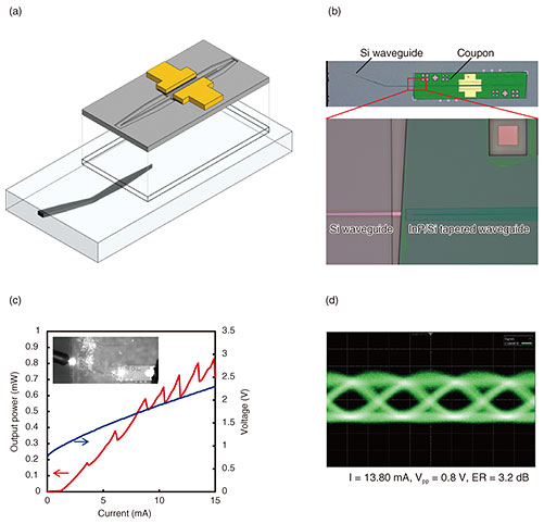
After the regrowth process, a lateral p-i-n junction is formed through silicon ion implantation and zinc diffusion, providing n-type and p-type doping, respectively (Fig. 2(d)). The InP surface is then slightly etched to form surface gratings, which serve as optical cavities (Fig. 2(e)). The InP membrane layers are vertically etched to form InP-based channel waveguides (Fig. 2(f)), followed by deposition of a silicon oxynitride (SiON) layer for surface coverage (Fig. 2(g)). Contact vias are opened through the SiON, and electrodes are deposited on top of the membrane and SiON (Fig. 2(h)). These steps complete the fabrication of the active III-V membrane. The final steps involve releasing the membranes by removing the sacrificial layers. First, the SiON mask is patterned and dry-etched into rectangular shapes, including alignment marks for the transfer process (Fig. 2(i)). The sacrificial layers are then wet-etched, using the SiON as a mask, until the InP substrate is exposed (Fig. 2(j)). The entire wafer is coated with photoresist and patterned to define tethers (Fig. 2(k)). Finally, the InAlAs sacrificial layers are wet-etched, leaving the III-V membranes supported solely by the photoresist tethers (Fig. 2(l)). At this stage, the III-V membranes are ready for pickup as coupons for micro-transfer printing. 3. Micro-transfer printing on silicon waveguidesOur initial demonstration of micro-transfer printing involved a DR laser integrated onto a silicon waveguide, as schematically shown in Fig. 3(a) [8]. First, we prepared SOI wafers and fabricated silicon waveguides with (1) taper sections for adiabatic mode conversion from the III-V membrane to silicon, (2) 20° single-mode bend waveguides to suppress facet reflections, and (3) tapered wide waveguides for efficient fiber coupling. The wafer surface was covered with silicon dioxide (SiO2) and planarized using chemical mechanical polishing to ensure a flat surface. III-V membrane coupons incorporating DR lasers [8] were then prepared. Each DR laser comprised a 140-µm-long DFB section and 60-µm-long distributed Bragg reflector (DBR) section, enabling selective light extraction from the front side of the DFB. We used InP-based rib waveguides—rather than channel waveguides as described in Section 2—for the initial trials. The structure of the rib waveguides is also depicted in Fig. 3(a). The coupons were then transferred onto the silicon waveguides, and Fig. 3(b) presents a microscopic image of the resulting chips. Since micro-transfer printing requires precise placement of coupons onto the target wafers, the optical-coupling scheme must be designed to accommodate potential alignment errors. We carefully engineered adiabatic mode converters between the coupons and silicon waveguides to ensure tolerance to misalignment. In the 50-µm-long tapered region, the width of the InP rib waveguide narrows from 1.0 to 0.1 µm, while the width of the silicon channel waveguide expands from 0.08 to 2.0 µm. Simulations indicated that this design provides a 1-dB tolerance for up to 0.6-µm misalignment, which is achievable with precise alignment stages. Cross-sectional transmission electron microscope (TEM) images of the fabricated chip revealed an actual misalignment of 0.45 µm. We characterized the fabricated devices by sweeping the injected current at a stage temperature of 25°C and measuring the output light using a spatial photodiode. Figure 3(c) shows the output power and applied voltage as functions of the injected current (light-current-voltage (L-I-V) characteristics). The devices exhibited a threshold current of 1.2 mA, comparable to those fabricated by conventional wafer-scale processes [9]. The maximum output power reached 0.8 mW. The inset of Fig. 3(c) displays an infrared image of the chip under operation. Finally, we demonstrated direct modulation of the device using a pulse pattern generator, bias tee, optical-to-electrical converter, and sampling oscilloscope. The output light was amplified using an erbium-doped fiber amplifier, and Fig. 3(d) shows the resulting eye diagram at a 40-Gbit/s non-return-to-zero (NRZ) data rate. A clear eye opening was observed with a bias current as low as 13.8 mA, attributed to strong optical confinement in the active region and the short-cavity design. The dynamic extinction ratio (ER) was measured to be 3.2 dB.
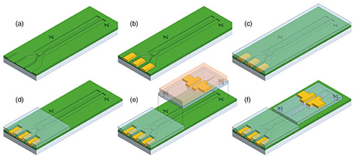
Although we successfully fabricated directly modulated lasers (DMLs) operating at high baud rates, the modulation speed was limited by the relaxation oscillation frequency inherent to DMLs. To overcome this limitation and further enhance the flexibility of the target substrate, we explored micro-transfer printing of lasers onto external high-speed modulators, as discussed in the following section. 4. Micro-transfer printing on TFLN platformLithium niobate has long been used as a material for optical modulators. Early implementations used titanium-diffused waveguides, which exhibited relatively large mode sizes. However, the advent of smart-cut technology has enabled the fabrication of TFLN wafers, enabling the fabrication of much more compact and high-speed modulators [10]. TFLN wafers have thus become an attractive platform for complex photonics integrated circuits. Consequently, there have been numerous efforts to integrate lasers onto TFLN platforms [11], including approaches such as flip-chip bonding of DFB lasers [12], heterogeneous integration [13], and photonic wire bonding [14]. A key challenge for these integrations is achieving low-loss optical coupling between the laser and TFLN waveguides. We demonstrated micro-transfer printing of DR lasers onto TFLN wafers to fabricate high-speed transmitters [15]. Figure 4 illustrates the process flow for fabricating TFLN waveguides, Mach-Zehnder modulators (MZMs), and subsequent micro-transfer printing. We began with x-cut TFLN wafers featuring 0.6-µm-thick TFLN layers. Waveguides were fabricated using previously reported processes [16], and the photonic circuit included Mach-Zehnder interferometers (MZIs), adiabatic optical couplers for the III-V coupons, and edge couplers (Fig. 4(a)). The waveguide etch depth was 0.4 µm. Chromium/gold (Cr/Au) electrodes were then deposited on both sides of the MZI to function as MZMs (Fig. 4(b)). Silicon dioxide was deposited as a cladding layer (Fig. 4(c)), and vias were dry-etched at the electrode locations to provide electrical contacts. Finally, the SiO2 was removed in regions designated for micro-transfer printing (Fig. 4(d)).
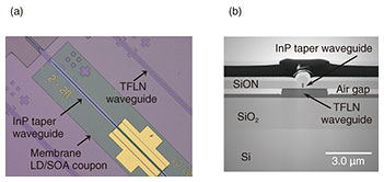
III-V DR laser coupons were fabricated on an InP wafer using the procedures detailed in Section 2. These DR lasers comprised a 200- or 140-µm-long DFB section and 80-µm-long DBR section, with an overall coupon size of 200 × 800 µm. The active region consisted of InGaAlAs-based MQWs with a photoluminescence peak at 1.26 µm. The DR-laser coupon was picked up from the host InP wafer and transferred to the prepared TFLN wafer (Fig. 4(e)). Finally, the tether resist was removed (Fig. 4(f)). Figure 5(a) presents a microscopic image of a DR laser transferred onto the TFLN substrate, successfully positioned within the locally opened region. Figures 5(b) and 5(c) show cross-sectional TEM images at the InP-TFLN coupling region and the MZM phase shifter arm, respectively. From the TEM analysis, the alignment error between the TFLN waveguide and the InP coupon was measured to be 0.15 µm.
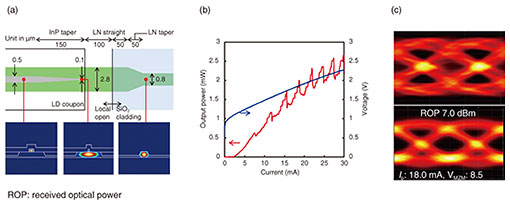
Designing optical couplers that are tolerant to alignment errors during transfer printing is crucial. Figure 6(a) depicts the detailed schematic of the coupling region and the corresponding optical modes. The width of the InP channel waveguide is tapered from 0.5 to 0.1 µm, while the width of the TFLN waveguide is initially 2.8 µm. This taper enables efficient mode conversion from the InP waveguide to the fundamental mode of the wider TFLN rib waveguide. Subsequently, the TFLN waveguide width is reduced from 2.8 to 0.8 µm. Simulations indicate that this design exhibits only a 0.5-dB excess loss for a 1.0-µm alignment error. Figure 6(b) shows the L-I-V characteristics of a transfer-printed DR laser, with a DFB section length of 200 µm, integrated onto a reference TFLN waveguide (without an MZM) at a stage temperature of 25°C. The device demonstrated a threshold current of 1.7 mA and maximum output power of 2.7 mW, as measured using a spatial optical power meter. We also integrated another DR-laser coupon, with a DFB section length of 140 µm, onto the TFLN MZM region. The MZM arm length was 8.0 mm. The DR laser was biased at 18.0 mA, and the TFLN MZM was driven using an arbitrary waveform generator operating at a 128-Gbit/s NRZ signal. The output light was coupled to a lensed fiber, detected with a uni-traveling carrier photodiode and analyzed with a digital storage oscilloscope after amplification with a praseodymium-doped fiber amplifier. Figure 6(c) displays the eye diagrams of the input electrical signal (top, without equalization) and output optical signal (bottom, after equalization with a 41-tap linear equalizer). A clear eye opening was observed from the TFLN MZM chip with the micro-transfer printed membrane DR laser. Bit error rate (BER) measurements in a back-to-back configuration yielded a BER below the KP-4 forward-error-correction threshold.
5. SummaryWe have demonstrated the micro-transfer printing of III-V membrane lasers onto various platforms, including silicon photonics and TFLN. Our III-V membrane lasers offer high modulation efficiency and enable straightforward optical coupling to the underlying platform via adiabatic tapers. On silicon, the integrated lasers achieved direct modulation at 40 Gbit/s with a bias current as low as 13.8 mA. By transferring the III-V membrane lasers onto TFLN MZMs, we attained even higher bit rates of up to 128 Gbit/s. We believe that micro-transfer printing will play a pivotal role in the integration of III-V devices onto diverse photonics platforms, enabling efficient utilization of source materials. References
|
||||||||||||||||||||||||||||||||||