|
|||
|
|
|||
       |
Feature Articles: Keynote Speeches at NTT R&D FORUM 2025―IOWN∴Quantum Leap Vol. 24, No. 3, pp. 20–28, Mar. 2026. https://doi.org/10.53829/ntr202603fa1  Innovation in Computing Powered by Photonic Technology―Evolution toward IOWN 2.0 and 3.0, and the Leap to QuantumAbstractThis article presents NTT’s research and development efforts toward innovation in computing powered by photonic technology. It is based on the keynote speech given by Akira Shimada, NTT president and chief executive officer, at the “NTT R&D FORUM 2025―IOWN∴Quantum Leap” held from November 19th to 26th, 2025. Keywords: IOWN, photonics-electronics convergence (PEC) device, optical quantum computer
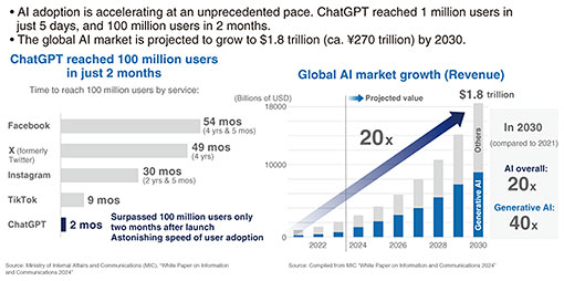
1. Innovation in computing powered by photonic technologyToday, I will introduce two major computing innovations enabled with NTT’s photonic technologies. The first is IOWN (Innovative Optical and Wireless Network) photonic computing. By replacing electrical wiring with optical wiring, we break through energy limitations and enable a low-power computing infrastructure for the artificial intelligence (AI) era. The second is an optical quantum computer. This technology surpasses the computational limits of conventional computers and solves previously intractable problems with dramatically lower power consumption. 2. IOWN photonic computingNTT supports the evolving “communications of the future” with “low power consumption through light,” with its IOWN Photonic Disaggregated Computing from both the hardware and software perspectives. In terms of hardware, electrical signals will be replaced with optical signals, reducing power consumption and achieving high-speed communication with low latency. In terms of software, large-scale computers that require advanced processing have traditionally had restrictions on the combination of parts, necessitating the installation of additional cabinets, which consumed power even for parts that were not being used. However, by removing these restrictions and using resource allocation technology that allows for only the necessary functions to be used in the amounts required, we have achieved more advanced processing and reduced power consumption. By combining this with the ultra-high-speed All-Photonics Network (APN), it will be possible to use computers in remote locations as if they were a single high-performance computer. This will enable efficient use of electricity near renewable energy sources and power-generation facilities. Through these technologies, NTT will support the evolving communications of the future with low power consumption through light. 2.1 Rapid advancement and expansion of AI utilizationAI utilization is expanding at an unprecedented pace. It once took Facebook 54 months to reach 100 million users, but OpenAI’s ChatGPT reached that same milestone in just 2 months. With this rapid expansion, the global AI market is projected to grow to USD 1.8 trillion by 2030 (Fig. 1).
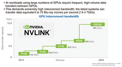
The scale of the computers used to develop and operate AI models is growing at a rate of about 1.8 times per year. In 2020, OpenAI’s GPT-3 system was equipped with roughly 10,000 graphics processing units (GPUs). By 2022, the GPT-4 system expanded to 25,000 GPUs. Today, the latest system being developed by another US company reportedly incorporates 200,000 GPUs. 2.2 The superiority of light in high-capacity communicationIn AI systems with large numbers of GPUs, enormous volumes of data must be exchanged between GPUs. As a result, inter-GPU communication bandwidth has grown sharply. NVIDIA’s latest GPUs support communication speeds of 14.4 terabits per second (Tbit/s) (Fig. 2). This is equivalent to transferring the data of 72 Blu-ray movies in 1 second.
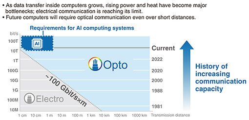
In such high-bandwidth environments, electrical wiring becomes significantly less efficient as transmission distance increases. With today’s massive data flows, even short connections of only a few tens of centimeters inside a computer can consume substantial power. In contrast, optical communication consumes almost no additional power even over longer distances. This is the advantage of light. Because of these differences, communication inside computers is reaching the limits of electrical wiring. Rising power and heat have become major bottlenecks. Figure 3 shows the regions where electrical and optical communications are suitable. As communication bandwidth increases, even short distances require optical communication. In the ultra-high-bandwidth communication required by today’s AI systems, we are clearly reaching limits of electrical communication, and optical communication is becoming the more suitable option.
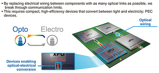
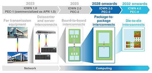
For more than 40 years, NTT has advanced research, development, and deployment of optical communication technologies, supporting the evolution of information networks. We began by connecting NTT central stations with optical links to achieve larger capacity and higher speed. Over time, we extended optical communication to homes and inside datacenters. We have continually innovated optical communication to meet the most advanced needs of each era. 2.3 Optical interconnection using photonics-electronics convergence devicesMost components inside computers, such as central processing units (CPUs) and GPUs, currently operate only on electricity and are interconnected by electrical wiring. However, as mentioned earlier, even over short distances, transmitting large volumes of data requires significant power. By replacing this electrical wiring with optical one, we can substantially reduce power consumption. However, simply replacing electrical wiring with optical wiring is not enough. Since processing components operate on electricity, signals must be converted between electrical and optical forms. We thus need compact and efficient devices for this conversion. We call such devices photonics-electronics convergence (PEC) devices. A PEC device is an integrated package containing all the functions needed to convert signals between light and electricity such as a photodiode, electrical amplifier, laser diode, and laser driver. To achieve photonic computing, each component inside the computer will require one of these devices. This requires making the device as small as possible and maximizing its power efficiency to avoid unnecessary energy consumption. Under the IOWN vision, we plan to enhance PEC devices in stages and extend their application from the network down into the computer itself. In IOWN 1.0, we applied our first-generation device, PEC-1, to network interconnects such as relay equipment, datacenter interconnects, and server-to-server links. The resulting high-speed, large-capacity, low-latency network service, APN IOWN 1.0, was commercialized in 2023. With IOWN 2.0, which began in 2025, we are finally applying these devices inside computers. Using the evolved PEC-2, we are replacing electrical wiring between computer boards with optical wiring (Fig. 4).
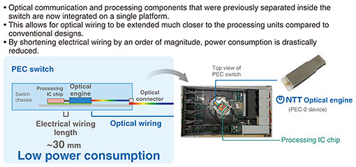
2.4 Devices enabling IOWN 2.0We are developing a PEC-2 device to deliver IOWN 2.0, with commercial availability planned for fiscal year 2026. It is a very compact device and is referred to as an optical engine. The optical communication switch (PEC switch) incorporates 16 PEC-2 devices, can transmit 102.4 Tbit/s, and offers performance fully suited for AI workloads. We demonstrated a computer operating at one-eighth the power consumption using the prototype version of these devices at the NTT Pavilion at Expo 2025 Osaka, Kansai, Japan. 2.5 Innovation with the optical engineIn conventional optical communication switches, optical modules were inserted at the front of the switch and connected via electrical wiring to the integrated circuit (IC) chips that executed switching and control. At roughly 300 mm, this long electrical wiring was a major contributor to increased power consumption. In the PEC switch, the optical engines and IC chips are mounted together on a single baseboard, allowing for optical wiring to be routed much closer to the processing IC chip. We have thus been able to reduce the length of the electrical wiring by roughly a factor of ten, to around 30 mm, and dramatically lower power consumption (Fig. 5).
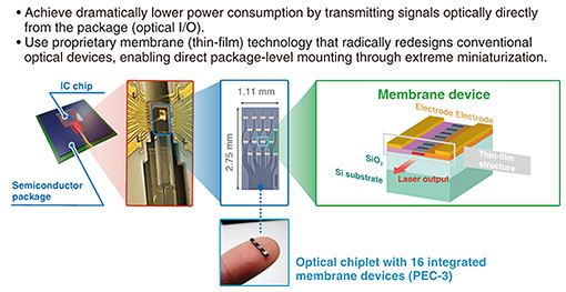
To bring the PEC switch to market, we have established partnerships across the global supply chain, including with Broadcom in the United States and Accton Technology in Taiwan. Within our own group, NTT Innovative Devices serves as the design and manufacturing hub for the core optical engine and switch modules and coordinates the overall system integration. Some may wonder if such high capacity is truly necessary. Broadcom’s Tomahawk 6 large-scale integrated circuit, which is used in datacenter switches, already processes 102 Tbit/s, confirming the need for optical wiring. NTT Innovative Devices is currently building a production capability of 5000 optical engines per month per manufacturing line. Going forward, we plan to expand to at least three lines, depending on demand. To enhance productivity, we are introducing advanced automation, such as robotics, into the assembly, packaging, and inspection processes. 2.6 IOWN 3.0: Further evolution of photonic computingIn IOWN 3.0, we will move beyond board-to-board optical connections introduced in IOWN 2.0 and, using the next-generation PEC-3 device, transition to optical connections directly between semiconductor packages such as CPUs and GPUs (Fig. 6). We will achieve dramatic power savings by transmitting information directly from packages via optical wiring (optical input/output (I/O)). To achieve this, it is necessary to shrink the PEC device to a size that can be directly attached to the package. To that end, NTT has fundamentally reinvented the structure of optical devices, developing a proprietary thin-film fabrication method known as the membrane device architecture. Our prototype optical transmitter module mounts 16 of these membrane devices onto an extremely compact “chiplet,” small enough to rest on the tip of a finger. We are accelerating research and development (R&D) on this PEC-3 optical chiplet as we move toward commercialization. We expect to begin offering commercial samples in 2028 (Fig. 7).
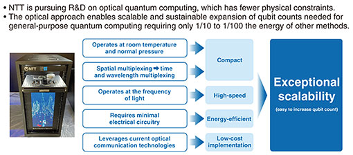
IOWN will continue to evolve even after 3.0. With IOWN 4.0, targeted for around 2032, we will begin optical interconnects inside the package, ultimately aiming for a hundredfold reduction in power consumption. IOWN represents more than 40 years of NTT’s optical R&D, and this body of innovation is now expanding beyond traditional telecommunications into the very heart of computing. 3. Optical quantum computerEven with the latest computer and AI technologies, critical problems remain, and interest in quantum computing is growing. Quantum computing research has advanced, ushering in a wave of industrialization. The quantum computing market is expected to grow to tens of billions of dollars by the 2030s. Expectations are higher than ever before. Quantum computing takes many forms—superconducting, neutral-atom, and optical. NTT is pursuing the optical approach, rooted in its optical communication technology. By harnessing the nature of light, it achieves high speed, low power, and extraordinary scalability. It naturally integrates with communications, connecting seamlessly with future networks. We are leading quantum computing to its next stage—through the power of light. This is a new computational foundation for a sustainable society as it maximizes energy efficiency. 3.1 Limitations of conventional computersConventional computers face a fundamental limitation when solving problems that require evaluating an enormous number of possible configurations. To use a simplified analogy: solving such a problem on a classical computer is like navigating a maze by checking one path at a time—following a corridor until reaching a dead end, backtracking to the last junction, and trying the next path until an exit is found. As the maze becomes more complex, the number of paths that must be checked grows explosively. In contrast, a quantum computer behaves as if it were exploring all paths at the same time then, through its processing, leaving only the path that leads to the exit. Because it can examine multiple possibilities simultaneously, it can drastically reduce the number of computation steps, enabling it to solve far more complex problems than conventional computers. 3.2 Expectations for quantum computersThere are real-world problems that have remained unsolved due to the limitations of conventional computers. Examples include optimizing traffic and logistics in large cities, solving food problems by efficiently synthesizing fertilizers, designing optimal drug molecular structures tailored to each person, and designing fusion reactors, which are expected to become new energy sources. Quantum computers are expected to make it possible to solve these types of problems. The source of this capability in quantum computers lies in a fundamentally different way of representing information, namely, through quantum bits or qubits. Conventional computers use bits that hold either 0 or 1. Because a bit must be in one definite state at any moment, a classical system can represent only one state at a time. Quantum computers, on the other hand, use qubits that can hold both 0 and 1 at the same time. Since one qubit can represent two states at the same time, the number of states that can be represented grows exponentially as the number of qubits increases. By executing operations on these qubits, a quantum computer can process multiple states at once. The number of qubits a quantum computer possesses directly determines the complexity of the problems it can solve. Systems with fewer than about 1000 qubits are mainly used for research and demonstrations rather than practical applications. With around 100,000 qubits, it becomes possible to solve medium-scale problems. However, to use quantum computers broadly for applications with major societal impact, between 1 and 100 million qubits will be required. 3.3 History of quantum computersThe concept of quantum computing was proposed in the 1980s. However, it took 35 years from that point to create a real quantum computer, which only had 5 qubits. Advances in semiconductor technology and increased investment have accelerated the expansion of qubit counts. However, achieving the scale of 1 million to 100 million qubits is still a distant goal. One reason expanding qubit numbers is challenging is the limitations of conventional approaches. Superconducting and neutral-atom systems require extreme conditions such as ultra-low temperatures and vacuum environments, necessitating large, complex equipment. These requirements have historically constrained the scalability of qubit counts. 3.4 Optical approachNTT has focused on the optical approach, which has fewer operational constraints, and is actively pursuing R&D in this area. Optical quantum computers offer advantages not present in conventional approaches, including operation at room temperature and atmospheric pressure, high speed, and low power consumption. The optical approach enables scalable and sustainable expansion of qubit counts needed for general-purpose quantum computing requiring only 1/10 to 1/100 the energy of other methods (Fig. 8).
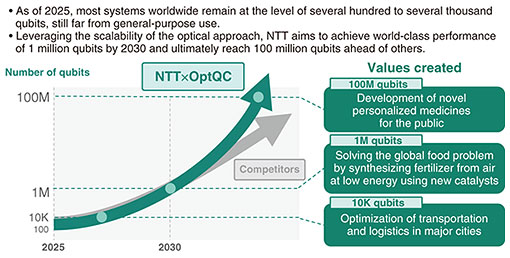
3.5 Roadmap to scale optical quantum computersWe have applied our long-standing optical technology research to create quantum light sources, generating light pulses with quantum properties, and in collaboration with OptQC, RIKEN, and others, developed an Internet-accessible optical quantum computer in 2024. NTT’s quantum light sources can generate light with exceptionally high-quality quantum properties. In other words, the “quantum yield” is high, which contributes to further improvements in scalability. This capability builds on technologies we have developed through advancing optical communications, including optical amplification and modulation of light properties. NTT and OptQC have signed a collaboration agreement aimed at the development of optical quantum computers. By combining NTT’s optical communication technology applicable to the quantum field with OptQC’s development technology for optical quantum computers, we aim to develop world-leading, scalable, and highly reliable optical quantum computers. Even at the current forefront of global research, qubit counts remain in the hundreds to a few thousand, far below the 1 million to 100 million qubits required for general-purpose use. NTT aims to leverage the scalable nature of optical quantum systems to achieve 1 million qubits at the world’s leading level by 2030. We also plan to take the lead in reaching 100 million qubits in the future (Fig. 9).
4. In conclusionNTT is using optical technologies to break through the limits of energy consumption and conventional computational processing, driving innovation in computing. The world is currently undergoing unprecedented transformation driven by AI, and NTT not only provides the infrastructure to support the AI era but also contributes to a sustainable future through innovation in computing for the forthcoming quantum era. |
||