|
|||||||||||||||||||||||||||||||||||||||||||||
|
|
|||||||||||||||||||||||||||||||||||||||||||||
       |
Regular Articles Vol. 24, No. 5, pp. 47–54, May 2026. https://doi.org/10.53829/ntr202605ra1 High-speed Vertical-illumination Photodiode for Beyond-200-Gbaud ApplicationsAbstractThe rapid increase in data traffic is pushing optical communication systems toward higher symbol rates. High-speed, high-responsivity photodiodes (PDs) are therefore essential for next-generation transceivers. We report on our fabricated vertical-illumination InP/InGaAs (indium phosphide/indium gallium arsenide) PD designed for symbol rates beyond 200 Gbaud, offering a 3-dB bandwidth over 100 GHz. By interference-based absorption enhancement, the PD exhibits responsivity exceeding 0.5 A/W over a broad absorption wavelength range. The inverted p-down structure enables electric-field confinement, resulting in a low dark current of approximately 1 pA with small device-to-device variation. These results indicate the suitability of the fabricated PD for future high-symbol-rate receivers. Keywords: high-speed photodiode, vertical illumination, inverted structure
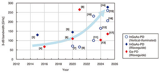
1. IntroductionRecent growth in data traffic driven by generative artificial intelligence (AI), cloud computing, and high-resolution video streaming, has accelerated the demand for higher-capacity optical links. Datacenter interconnect components are already moving toward 100-Gbaud-class operation, and further scaling to 200–400 Gbaud is expected for next-generation Ether-net systems [1]. High-speed photodiodes (PDs) are also attracting interest for photonic wireless links, including beyond-5G (fifth-generation mobile communications) and sub-THz applications [2], highlighting their importance across both fiber-optic and photonic-wireless platforms. Research on PD bandwidth has accelerated, as summarized in Fig. 1 [3–17]. For 200-Gbaud signaling, receiver PD bandwidths well above 100 GHz are typically required, which have been demonstrated using indium gallium arsenide (InGaAs) [3, 5, 7, 9–12, 14–16] and germanium (Ge) absorbers [4, 6, 8, 13, 17]. Relaxing the trade-off between bandwidth and responsivity remains a critical challenge in PD design. As the absorber volume is reduced to shorten the carrier transit time and resistance-capacitance (RC) time constant, the optical absorption decreases, leading to lower responsivity. Simultaneously improving bandwidth and responsivity is critical because it directly enhances receiver sensitivity, supporting longer transmission reach and improved optical signal-to-noise ratio.
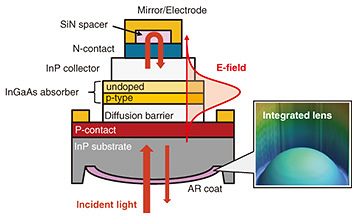
Waveguide-coupled PDs are widely used for high-speed, high-sensitivity detectors. In these devices, the absorber stacking direction is orthogonal to the light propagation direction, which maintains the optical absorption length even when a thin absorber is used, enabling both high absorption and short carrier transit times. Numerous waveguide PDs with bandwidths exceeding 100 GHz have been reported [3, 5, 6, 8, 13, 14, 17]. However, their external responsivity is often constrained by fiber-to-waveguide coupling loss. Typical issues include high polarization-dependent loss [5] and large dark current [8]. In contrast, vertical-illumination PDs, in which the absorber stacking direction is aligned with the propagation direction of incident light, offer several attractive features, including reduced optical coupling loss and suppression of surface-related dark currents [7]. These characteristics provide effective solutions to the above issues [7, 9–12, 15, 16]. We previously reported a vertical-illumination PD with a 70.1-GHz bandwidth and 0.61-A/W responsivity, where electric-field confinement improved dark current and reliability [7]. We have also reported vertical-illumination unitraveling-carrier (UTC) PDs with 3-dB bandwidths beyond 300 GHz [18]. However, achieving high responsivity in vertical-illumination PDs is generally challenging because absorber thinning, used to increase speed, typically results in a large responsivity penalty. Several approaches have been reported to enhance both responsivity and bandwidth. Resonance-based enhancement can improve responsivity without major structural modifications; however, it typically introduces strong wavelength dependence [19]. We fabricated a vertical-illumination PD with a monolithically integrated indium phosphide (InP) microlens [12]. The PD exhibited a high 3-dB bandwidth of 165 GHz owing to a small mesa diameter of 8 μm and thin absorber of 300 nm. A responsivity of 0.53 A/W at 1550 nm was also achieved by introducing a silicon nitride (SiN) spacer and top-mirror structure to maximize absorption in the InGaAs absorber through multilayer thin-film interference over a wide wavelength range. By leveraging a highly refined process technology used in commercial products, the PD exhibits a low dark current of approximately 1 pA with high reproducibility. 2. Device structureFigure 2 illustrates the cross-sectional structure of the fabricated inverted p-down triple-mesa PD. The fundamental structure is consistent with the PD and avalanche photodiode technologies we have previously reported [20]. The epitaxial stack comprises a p-type contact layer, diffusion barrier, hybrid absorption layer composed of p-type InGaAs and undoped InGaAs (ud-InGaAs), InP collector layer, n-type contact layer, SiN spacer, and gold (Au) mirror, all grown on an InP substrate.
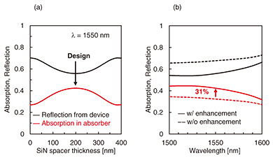
Reducing the sheet resistance of the p-type contact layer and the contact resistance at the semiconductor-electrode interfaces is essential for high-speed operation. The PD uses a small n-contact mesa diameter (8 μm) and thin absorber (300 nm) to reduce junction capacitance and the carrier transit time. Photoexcited electrons in the absorber are efficiently transported to the n-contact side by the conduction-band offset between the wide-gap diffusion barrier and InGaAs layer. The absorber comprises a hybrid layer of p-type InGaAs and ud-InGaAs, where the thickness ratio of the p-type absorber is optimized to maximize the 3-dB bandwidth. The ud-InP collector layer (170 nm) increases the depletion width and reduces capacitance. Overall, the layer structure is designed to maximize bandwidth as determined by the carrier transit time and RC time constant. Incident light is reflected multiple times by the metal mirror and multilayer stack, which modulates the electric-field intensity within the absorber. A monolithic InP microlens is incorporated on the back side of the thinned substrate to increase the effective optical aperture and ease alignment and mounting [9]. An anti-reflection (AR) coating is also deposited to suppress surface reflection. The microlens is smooth and has an approximately parabolic profile, as shown in a three-dimensional (3D) image obtained with a confocal laser scanning microscope (Fig. 2 inset). 3. Interference-based absorption enhancementFigure 3 shows the calculated absorption and reflection in the multilayer stack of the fabricated PD. The electric-field intensity in the absorber is modulated by interference in the multilayer structure (Fig. 2), which arises from multiple reflections at layer boundaries and at the metal mirror. The total absorption can be further increased by optimizing the thickness of each layer and adjusting the interference phase. However, the semiconductor layer thicknesses cannot be designed independently because they are constrained by carrier transit time, capacitance, and baseline absorption. Therefore, we adjusted the phase by designing the SiN spacer thickness to be 200 nm, thus enhancing absorption in the InGaAs absorber (Fig. 3(a)).
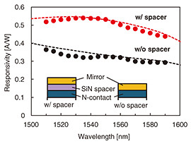
A trade-off exists between peak responsivity and the usable absorption wavelength range. Because the fabricated PD exhibits relatively low reflectivity at internal interfaces, the simulations show a broad absorption spectrum and increased responsivity (31% relative to calculations without interference) (Fig. 3(b)). The broad absorption also indicates robustness to fabrication errors. For example, even a 20% variation in the SiN spacer thickness results in a responsivity reduction of less than 3%. Figure 4 shows the measured wavelength dependence of responsivity. Under a 2-V reverse bias, the measured responsivity is consistent with simulations that account for interference-based absorption enhancement from multiple reflections in the C-/L-band (red dashed line). The responsivity is 0.53 A/W at 1550 nm and exceeds 0.5 A/W across the entire C-band.
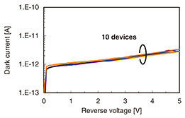
To clarify the contribution of interference-based absorption enhancement, we also fabricated a PD without a SiN spacer. This reference device exhibited a lower responsivity of 0.32 A/W at 1550 nm (black line), providing experimental evidence that the interference-based design significantly improves responsivity. 4. Dark-current characteristics of the inverted structureIn the inverted p-down structure, the electric field is confined to the region between the n-contact and p-contact layers, and the field along the absorber sidewalls is substantially suppressed compared with that inside the PD. This configuration significantly reduces surface-related dark current. A key feature of this triple-mesa structure is that it can be fabricated using only semiconductor epitaxial growth and multi-step wet etching, without ion implantation and the diffusion technique required for planar-type PDs. Eliminating these processes requiring high processing temperatures improves the controllability and reproducibility of the doping profile, leading to stable device fabrication. Figure 5 shows dark-current characteristics for ten PDs with an 8-μm active-area diameter fabricated on the same wafer. The PDs exhibit a dark current of approximately 1.3 ± 0.1 pA at 2 V. This low dark current is among the lowest reported for PDs and supports high reliability. These results reflect the expected effect of electric-field confinement in the fabricated inverted p-down structure.
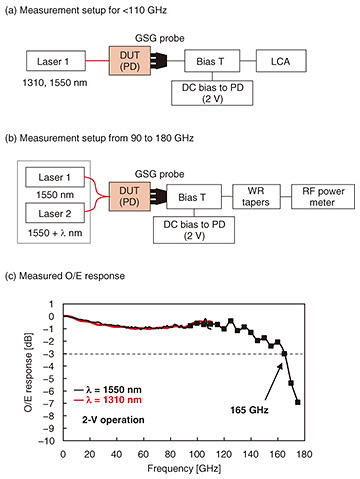
5. High-speed performanceFigures 6(a) and (b) show the experimental setups for measuring the optical-to-electrical (O/E) response of the fabricated PD. The measurements were conducted at wavelengths of 1550 nm (black) and 1310 nm (red) from 0.1 to 110 GHz using a lightwave component analyzer (LCA). A ground-signal-ground (GSG) probe was connected to the device under test (DUT) with a 1-mm connector, and a reverse bias was applied through a bias tee. The O/E response beyond 90 GHz at 1550 nm was measured using a heterodyne technique [8]. In this measurement, the generated radio frequency (RF) signal corresponds to the difference frequency between Laser 1 (fixed at 1550 nm) and a tunable laser (Laser 2). The O/E response was obtained by sweeping the wavelength of Laser 2 while monitoring the RF power. The GSG probe was connected to a hollow metallic waveguide tailored to the measurement frequency, and the signal was transmitted through a waveguide taper (WR taper) to an RF power meter. Figure 6(c) shows the measured O/E response (normalized at 0.1 MHz) at a bias voltage of 2 V. The response roll-off up to 110 GHz was within −1 dB, and the 3-dB bandwidth reached approximately 165 GHz at 1550 nm. Although heterodyne measurements were not conducted at 1310 nm due to limitations of this experimental setup, the O/E response at 1310 nm was confirmed to match that at 1550 nm up to 110 GHz.
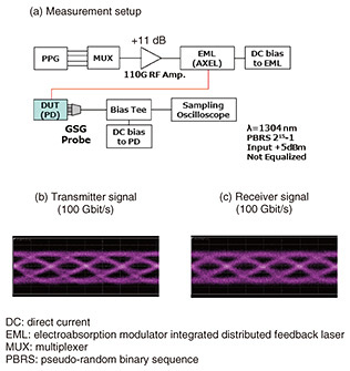
Figure 7(a) shows the experimental setup for measuring an eye diagram of a 100-Gbit/s non-return-to-zero (NRZ) signal at a bias voltage of −2 V. The electrical signal from a pulse pattern generator (PPG) was amplified and used to drive a semiconductor-optical-amplifier-assisted extended-reach electroabsorption modulator-integrated distributed feedback laser (AXEL) module [21], the optical launch power and 3-dB bandwidth of which were +5 dBm and approximately 66 GHz, respectively. The PD output was captured using a sampling oscilloscope without equalization. Figures 7(b) and (c) show eye diagrams of 100-Gbit/s NRZ signals for the transmitter and receiver, respectively. The transmitter and receiver signals were evaluated using a reference UTC-PD with a 90-GHz bandwidth and the fabricated PD, respectively. Although the measurements were limited to 100 Gbit/s due to the available equipment, the received eye closely reproduced the transmitter eye, indicating a significant margin in the receiver bandwidth.
PDs designed for high-power operation typically use UTC absorbers rather than hybrid absorbers. In the fabricated PD, a hybrid absorber was used to prioritize high-frequency performance over high-power operation. Nevertheless, the PD exhibited no current saturation at an input power of +5 dBm. The results presented in this article suggest that the fabricated PD has strong potential for high-symbol-rate applications. 6. SummaryWe demonstrated a high-speed vertical-illumination InP/InGaAs PD achieving a 165-GHz 3-dB bandwidth together with 0.53-A/W responsivity by combining device scaling with interference-based absorption enhancement. Compared with conventional resonant-cavity-enhanced PDs, the fabricated PD provides a broader absorption wavelength range. The inverted p-down structure further enables low dark current and small fabrication variation. These results indicate that the fabricated PD is promising for future high-symbol-rate applications. References
|
||||||||||||||||||||||||||||||||||||||||||||