|
|||||||||||||||||||||
|
|
|||||||||||||||||||||
       |
Feature Articles: Forefront Research on Ultrawide-bandgap Semiconductors Vol. 24, No. 6, pp. 14–20, June 2026. https://doi.org/10.53829/ntr202606fa1 Overview of Ultrawide-bandgap Semiconductor Research at NTTAbstractUltrawide-bandgap semiconductors exhibit high breakdown voltage, high-frequency operation, and excellent environmental robustness. They therefore have attracted significant attention as key materials for attaining a sustainable society and enabling next-generation innovative devices and systems. At NTT Basic Research Laboratories, we have been promoting research and development on aluminum nitride, cubic boron nitride, and diamond, using advanced crystal growth technologies developed through long-term studies on fundamental materials. We present the recent progress and future prospects of ultrawide-bandgap semiconductors. Keywords: aluminum nitride, cubic boron nitride, diamond
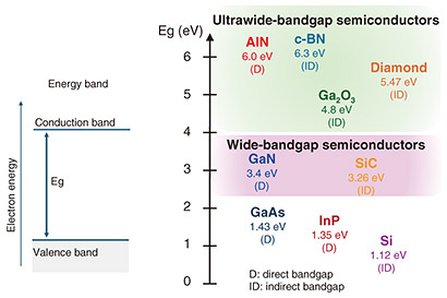
1. Untapped potential of semiconductorsSemiconductors are fundamental technologies that support the processing, conversion, and transmission of information and energy and used in a wide variety of applications in many fields. Integrated circuits in smartphones and personal computers execute information processing, while light-emitting diodes (LEDs) and laser diodes (LDs) convert electrical energy into light, solar cells convert light into electrical energy, and power devices are used in power supply/conversion and motor control. These semiconductor devices are key technologies directly contributing to improving energy efficiency. Computational resources, particularly those in datacenters, have increased significantly with the rapid advancement in artificial intelligence, further emphasizing the importance of semiconductors. As photonics–electronics convergence, represented by IOWN (Innovative Optical and Wireless Network), continues to evolve, the role of semiconductor devices operating at the interface between photonics and electronics is expected to expand. The field of semiconductors still holds substantial untapped potential. One promising area is ultrawide-bandgap semiconductors, which are the focus of this collection of feature articles. As they are relatively new semiconductor materials, they still present many unexplored challenges, ranging from fundamental physical properties to device process technologies and device design. In other words, continued advances in both material and technology development could lead to devices and systems that surpass current technological paradigms. In this article, we first review the fundamental concept of the bandgap and the principles of material selection then introduce the significance of ultrawide-bandgap semiconductors. 2. Ultrawide-bandgap semiconductors2.1 Bandgap: A key metric that determines semiconductor performanceOne of the fundamental material parameters that determines the properties of semiconductors is bandgap energy. Each semiconductor material has its own characteristic bandgap energy (Fig. 1). Materials with a bandgap energy close to 0 eV behave as conductors, enabling electrical current to flow easily, whereas materials with larger bandgap energies become increasingly insulating. Semiconductors lie between these extremes and are distinguished by their ability to control electrical conductivity over a wide range through impurity doping.
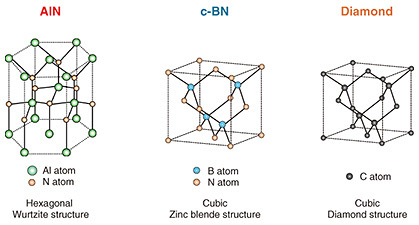
Semiconductors in which electrons (negative charge) are the dominant carriers are called n-type semiconductors, while those in which holes (positive charge) dominate are called p-type semiconductors. By controlling these carriers, devices such as transistors and diodes can operate, enabling information processing and power control. The bandgap energy is also crucial for optical functionality. In light-emitting devices, such as LEDs and LDs, light is emitted when electrons and holes recombine, and the emission wavelength is determined by the bandgap energy. Similarly, in solar cells that convert light into electricity, the range of absorbed wavelengths is governed by the bandgap energy. A larger bandgap energy generally corresponds to shorter emission and absorption wavelengths. Silicon (Si), the foundation of modern electronics, has a bandgap energy of 1.12 eV, which lies in a range suitable for controlling electrical conductivity. Silicon carbide (SiC, 3.26 eV) and gallium nitride (GaN, 3.4 eV), which have wider bandgaps (larger bandgap energies), are known as wide-bandgap semiconductors. Although wider bandgaps make conductivity control more challenging, decades of research and development have enabled their widespread use in visible LEDs, high-frequency transistors, and power devices. Materials with even larger bandgap energies include gallium oxide (Ga2O3, 4.8 eV), diamond (5.47 eV), aluminum nitride (AlN, 6.0 eV), and cubic boron nitride (c-BN, 6.3 eV). These materials are referred to as ultrawide-bandgap semiconductors and are being increasingly studied worldwide. Since each semiconductor has its own bandgap energy, materials are selected according to their intended applications. Differences in constituent elements and crystal structures (Fig. 2) also lead to variations in bandgap energy as well as in key physical properties such as breakdown electric field (voltage tolerance), thermal conductivity (heat dissipation capability), and electron saturation velocity (high-frequency performance). These properties determine the application domains in which each material excels. In this sense, selecting semiconductor materials can be considered a step in designing material properties.
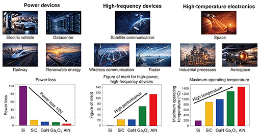
2.2 Application domains enabled by ultrawide-bandgap semiconductorsUltrawide-bandgap semiconductors are a class of materials with exceptionally large bandgap energies, offering advantages such as high breakdown voltage, high-frequency operation, robustness under harsh environments, and light emission in ultraviolet (UV) regions. We outline four key application areas in which these advantages are particularly significant. The first area is power devices (Fig. 3), which are widely used in applications ranging from home electronics and personal computers to datacenters, electric vehicles, railways, and renewable energy systems. Reducing power loss is a critical challenge in achieving carbon neutrality. Semiconductors with larger bandgap energies generally exhibit higher breakdown electric fields, making them advantageous for high-voltage and low-loss operation. While wide-bandgap semiconductors such as SiC and GaN are already being commercialized, the use of ultrawide-bandgap materials such as AlN and c-BN with even higher breakdown fields could further reduce power-conversion losses.
The second application of ultrawide-bandgap semiconductors is high-frequency transistors. These devices are key components in high-frequency power amplifiers used in wireless communication, satellite communication, and radar systems. Higher output power and operating frequency enable wider communication coverage and faster data transmission. Therefore, semiconductor materials must simultaneously exhibit high breakdown electric fields and high electron saturation velocities. While GaN is widely used in fifth-generation mobile communication systems (5G), ultrawide-bandgap materials capable of higher output power are garnering more attention for beyond-5G applications. In particular, AlN and c-BN combine high breakdown fields with high electron saturation velocities, making them highly promising for high-power, high-frequency applications. The third application is electronics for harsh environments. In conventional semiconductors, such as Si, intrinsic carriers generated by thermal excitation increase at high temperatures, causing leakage current even in the off state and making stable circuit operation difficult. Datacenters thus require a significant amount of energy for cooling. Materials with larger bandgap energies suppress the generation of intrinsic carriers, enabling operation at elevated temperatures and paving the way for high-temperature electronics. These materials are also expected to exhibit high radiation tolerance, expanding potential applications in extreme environments such as aerospace, nuclear energy, deep underground systems, and decommissioning of nuclear facilities. The fourth application is UV photonics. The UV region, particularly the deep-UV region, has long been a challenging and largely unexplored area for semiconductor light sources such as LEDs and LDs. However, materials with large bandgap energies are well suited for short-wavelength light emission and can serve as the basis for UV LEDs and LDs. Ultraviolet light has a wide range of applications, including sterilization and other medical uses, environmental purification, materials and chemical analysis, and microfabrication. It is also useful for solar-blind communication and sensing, which are less affected by sunlight. Unexplored materials may host new physical phenomena and functionalities that cannot be anticipated from current semiconductor technologies. At NTT Basic Research Laboratories, we are advancing research and development on the ultrawide-bandgap semiconductors AlN, c-BN, and diamond, with the aim of creating next-generation semiconductor technologies. 3. NTT’s ultrawide-bandgap semiconductor technologies3.1 Aluminum nitrideNTT Basic Research Laboratories was the first to develop an AlN semiconductor [1]. Aluminum nitride has a wide bandgap energy of approximately 6.0 eV and is the only ultrawide-bandgap semiconductor suitable for light-emitting devices due to its direct bandgap structure. Aluminum nitride has a hexagonal wurtzite crystal structure (Fig. 2), the same as that of GaN. Its alloy with GaN, AlGaN, can be formed stably over the entire composition range. By controlling the composition, the bandgap can be engineered over a wide range from 6.0 eV (AlN) to 3.4 eV (GaN). Therefore, advanced device structures, such as heterostructures, superlattices, quantum wells, and compositionally graded layers, can be used, providing high flexibility in device design. Because AlN-based semiconductors have bandgap energies corresponding to the UV region, they have been actively studied for applications in UV LEDs and LDs [2]. In addition, AlN exhibits excellent physical properties, including a high breakdown electric field, high thermal conductivity, and high electron saturation velocity, making it optimal for high-voltage, high-frequency, and high-temperature electronic devices. We have steadily expanded AlN-based device applications through continuous development of high-quality crystal growth, conductivity control, and device fabrication technologies. The article “AlN Transistors for Ultrahigh-temperature Electronics” in this issue [3] focuses on the operation of AlN transistors under extreme high temperatures. Thermally generated carriers increase at elevated temperatures, leading to leakage current even in the off state and degradation of the current on/off ratio, a key switching-performance metric. Due to its large bandgap energy, AlN has been theoretically predicted to maintain clear on/off states even at extremely high temperatures. The experimental results presented in the article indicate that AlN transistors can operate at temperatures as high as 1000°C and exhibit superior on/off ratios compared with that of other materials. The article “High-frequency Operation of AlN-based Polarization-doped Transistors” [4] addresses the development of AlN-based transistors for high-frequency applications. Conventional impurity doping is ineffective in high-Al-composition regions, making it difficult to form low-resistance channels. To overcome this challenge, polarization doping, which uses the intrinsic polarization properties of nitride semiconductors, was used to achieve high carrier densities even in high-Al-composition AlGaN. The article explains the principle of polarization doping and presents high-frequency characteristics extending into the millimeter-wave range. The article “AlN-based Deep-ultraviolet Laser Diodes” [5] presents the development of deep-UV LDs. Deep-UV light sources are expected to enable applications in sterilization and medical treatment, environmental purification, spectroscopic analysis, and solar-blind communication. In deep-UV LDs, efficient carrier injection into the light-emitting layer (active layer) and reduction in electrical resistance are critical for emission efficiencies. The article introduces a device structure with reduced resistance enabled using advanced crystal growth techniques and demonstrates deep-UV laser oscillation. The article “Gigahertz Acoustic Wave Devices Using AlN Piezoelectric Thin Films” [6] focuses on acoustic-wave devices featuring AlN piezoelectric films. In addition to being a semiconductor, AlN is also a piezoelectric material that can generate and detect mechanical vibrations (acoustic waves) under applied voltage. The article describes the development of high-speed gigahertz acoustic-wave devices using high-quality AlN thin films, as well as the exploration of novel physical phenomena arising from interactions between acoustic waves and electronic or spin degrees of freedom. 3.2 Cubic boron nitrideCubic boron nitride has the largest bandgap energy (approximately 6.3 eV) among ultrawide-bandgap semiconductors and predicted to have an extremely high breakdown electric field. Therefore, like AlN, c-BN has strong potential for power and high-frequency device applications. However, c-BN is a metastable phase and is challenging to synthesize; thus, the development of single-crystal thin films has been a major technical hurdle. We have developed a proprietary ion-beam-assisted molecular beam epitaxy technique, enabling the epitaxial growth of single-crystal c-BN thin films. Electrical conductivity control through Si impurity doping has also been achieved, paving the way for semiconductor applications of c-BN [7]. The article “Engineering of Novel Ultrawide-bandgap Nitride Semiconductors” [8] presents the crystal growth of cubic boron scandium nitride, a new c-BN-based ternary alloy. Cubic-boron-nitride-based alloys offer the advantage of tunable physical properties through composition control and are expected to serve as a material platform for future heterostructure devices. The creation of new materials expands the possibilities for device designs, which is one of the main goals of this research. 3.3 DiamondDiamond is distinguished not only by its excellent properties as an ultrawide-bandgap semiconductor but also by its superior spin properties. “Spin” refers to the degree of freedom corresponding to the magnetic orientation of electrons, and technologies that use spin as an information carrier are known as spintronics. Thus, diamond is attracting attention as a semiconductor material because its spin states are expected to be highly stable. We have been advancing research toward spin device applications based on thin-film synthesis technologies centered on plasma chemical vapor deposition, along with accumulated expertise in doping and electrode-fabrication processes. The article “Diamond Semiconductors for Spintronic Device Applications” [9] focuses on an approach for spin injection into diamond. In this study, the Schottky barrier formed at the interface between a ferromagnetic metal and diamond was used as a tunneling barrier. The article reports on the elucidation of the current transport mechanism in diamond Schottky barrier diodes using a permalloy alloy, which is a representative ferromagnetic material, as the Schottky electrode. These results establish a technological foundation for spin injection into diamond and may lead to further advances from the understanding of spin properties to the actualization of quantum functionalities. 4. Future prospectsDespite the outstanding physical properties of ultrawide-bandgap semiconductors, many aspects of their fundamental properties remain insufficiently understood. Therefore, deeper insight into materials, interfaces, and defects is essential. Because the characteristics of these materials still need to be clarified, current technologies cannot simply be extended or combined. It is necessary to develop new technologies while establishing an integrated approach spanning crystal growth, device process, and circuit and system design. In this process, in addition to the continuous accumulation of fundamental research, collaboration with universities, research institutions, and industry will play an important role. Ultrawide-bandgap semiconductors are promising next-generation materials not only for UV light-emitting devices but also for high-power, high-frequency, and environmentally robust electronic devices. Although AlN-based devices are still in the early stages of demonstration, their research and development are expected to accelerate. This is because current technologies developed for and knowledge gained on GaN-based devices can be leveraged, the current fabrication infrastructure can be used, and significant progress is being made in the development of large-diameter, high-quality AlN wafers. In emerging research areas such as c-BN-based alloys and diamond spintronics, it is essential to advance both material creation and the understanding of physical properties in parallel to fully use the potential of ultrawide-bandgap semiconductors. Through continued exploration of new application domains and advancements in device technologies, we aim to contribute to a sustainable society and the creation of future innovative devices and systems. References
|
||||||||||||||||||||