|
|||||||||||||||||||||
|
|
|||||||||||||||||||||
       |
Feature Articles: Forefront Research on Ultrawide-bandgap Semiconductors Vol. 24, No. 6, pp. 21–26, June 2026. https://doi.org/10.53829/ntr202606fa2 AlN Transistors for Ultrahigh-temperature ElectronicsAbstractAluminum nitride (AlN) is attracting significant attention as a semiconductor material able to operate in ultrahigh-temperature environments. We outline potential applications of high-temperature electronics and highlight the advantages of AlN for such applications. We also describe the development of AlN metal-semiconductor field-effect transistors at NTT, which can operate stably at temperatures as high as 1000°C. These devices exhibit the highest current on/off ratio reported to date for semiconductor transistors operating at such high temperatures, highlighting the strong potential of AlN for electronics in harsh environments. Keywords: aluminum nitride (AlN), high-temperature electronics, ultrawide-bandgap semiconductors
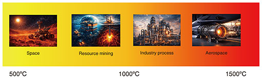
1. Semiconductor device applications in high-temperature environmentsSemiconductor devices able to reliably operate in high-temperature environments are attracting increasing attention (Fig. 1). One of the most important applications of high-temperature electronics is sensing. For example, if temperature and/or pressure can be measured directly in high-temperature regions, the operating conditions of equipment and industrial processes can be monitored more accurately. Conventionally, sensors and signal-processing circuits must be located away from high-temperature regions, and measurements are often conducted through long cables, which can cause response delays and electrical noise. In contrast, semiconductor devices that can stably operate at high temperatures enable direct sensing in harsh environments, improving both response speed and measurement accuracy.
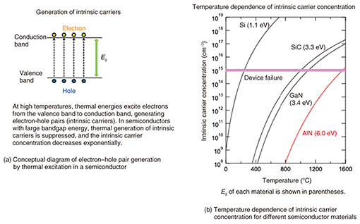
High-temperature device operation is also important in power electronics. In high-power applications, such as inverters for electric-vehicle motor drives and power circuits for datacenters, large amounts of heat are generated during operation. Therefore, electronic devices such as transistors and diodes need to operate stably at elevated temperatures. However, semiconductors consisting of conventional materials such as silicon (Si) exhibit degraded performance and unstable operation at high temperatures. Therefore, the application of semiconductor devices in high-temperature environments has been limited. 2. Features of ultrawide-bandgap semiconductor AlNAluminum nitride (AlN) has attracted considerable attention as a promising semiconductor material for high-temperature device applications. In conventional semiconductor materials, such as Si, electrons in the valence band are thermally excited into the conduction band at high temperatures. The closer the thermal energy is to the bandgap energy, the more intrinsic carriers*1 are generated (Fig. 2(a)). As the intrinsic carrier concentration increases, current becomes difficult to control in semiconductor devices. In a field-effect transistor (FET), the off-state leakage current due to thermally generated intrinsic carriers becomes excessively large, and the drain current can no longer be controlled by the gate voltage. This is one of the main reasons semiconductor devices based on conventional materials cannot be used in high-temperature environments. In contrast, AlN is an ultrawide-bandgap semiconductor*2 with a very large bandgap energy (Eg)*3 of 6 eV. A wider bandgap requires greater energy for thermally exciting electrons, thus suppressing the intrinsic-carrier generation even at high temperatures. Therefore, AlN FETs are expected to maintain the controllability of the drain current by the gate voltage even in high-temperature environments. As shown in Fig. 2(b), the intrinsic carrier concentration of Si exceeds 1 × 1015 cm−3 at around 200°C, making stable device operation difficult. In contrast, the intrinsic carrier concentration of AlN remains below 1 × 1015 cm−3 even at temperatures as high as 1400°C. This indicates that AlN-based semiconductor devices could operate at extremely high temperatures, which is difficult for semiconductor devices based on conventional materials.
In addition to its wide bandgap, AlN also exhibits excellent chemical stability and is resistant to oxidation and degradation at high temperatures. Therefore, its material properties remain stable even under extremely severe temperature conditions. Due to its strong interatomic bonding, AlN is predicted to have excellent radiation tolerance. Thus, radiation-induced crystal defects, which typically degrade semiconductor device performance, are less likely to form in AlN. This property is particularly advantageous for applications in radiation-rich environments such as outer space and nuclear power plants. Another important property of AlN is its extremely high breakdown electric field*4, which enables devices to withstand high voltages. This characteristic also makes AlN a promising material for power electronics.
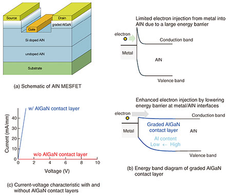
3. Development of AlN transistorsTo apply the excellent material properties of AlN to practical semiconductor devices, several technical challenges must be addressed. In this section, we describe our fabrication of AlN metal-semiconductor FETs (MESFETs)*5 (Fig. 3(a)) and the key process technologies developed for this study. One major challenge is forming low-resistance electrical contacts between the AlN channel layer and source and drain electrodes. Because AlN has a very large Eg, a high energy barrier forms at the interface between AlN and the electrode metal. This barrier prevents efficient carrier injection from the metal into the AlN channel. To overcome this issue, a compositionally graded aluminum gallium nitride (AlGaN) contact layer was introduced in the source and drain regions (Fig. 3(b)). In this structure, the Al content in AlGaN gradually changes from AlN to AlGaN with lower Al content toward the electrode side. This graded layer reduces the energy-barrier height between the metal electrode and AlN channel layer, enhancing carrier injection from the electrode into the AlN channel (Fig. 3(c)). Good ohmic contacts*6 can thus be obtained in AlN MESFETs [1].
A Schottky contact*7 at the gate electrode is also important for AlN MESFETs. If a large leakage current flows from the gate electrode to the AlN channel layer, the controllability and reliability of the device deteriorate significantly, particularly in high-temperature environments. In this study, nickel (Ni) was used as the gate electrode because of its large Schottky barrier height of ~3 eV on the AlN surface. This large barrier height effectively suppresses the gate-leakage current, resulting in excellent gate controllability of the drain-source current. These technological developments enabled our successful fabrication of AlN MESFETs with excellent device performance.
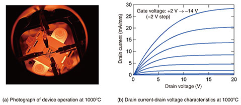
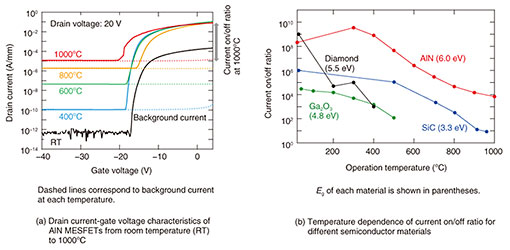
4. High-temperature operation of AlN transistorsTo investigate the stability of transistor characteristics at high temperatures, we fabricated AlN MESFETs, as described in the previous section (Fig. 3(c)), and constructed a high-temperature measurement system that enables heating up to 1000°C (Fig. 4(a)). The device wafer was placed inside a heating furnace, and electrical measurements were conducted by directly contacting probes with the electrodes of our AlN MESFETs under high-temperature conditions. Such a measurement system is technically challenging to establish, and transistor characterization at temperatures as high as 1000°C has rarely been reported for conventional semiconductor devices. Even at a high temperature of 1000°C, our AlN MESFETs show excellent pinch-off characteristics with a threshold voltage of −14 V (Fig. 4(b)). Demonstrating device operation at 1000°C, which has not been achieved with conventional semiconductor materials, represents an important milestone, highlighting the exceptional thermal stability of AlN as a device material. Interestingly, the on-state drain current above the threshold voltage increases as temperature increases for our AlN MESFETs (Fig. 5(a)). This temperature dependence of the drain current is opposite to that of conventional transistors in which the electron concentration remains almost constant at high temperatures, while electron mobility decreases due to phonon scattering. The drain current thus decreases as the temperature increases. In contrast, in AlN, the electron concentration exponentially increases with temperature due to the enhanced ionization of Si donors.
Another important feature is that, below the threshold voltage of −14 V, the off-state drain current remains low even at high temperatures, enabling clear on/off switching operation. Even at 1000°C, the current on/off ratio*8 is as high as 104. Although this value is sufficiently high, it is underestimated due to increased background current from the measurement system under high-temperature conditions. At high temperatures, the resistance of insulating materials used in cables, probes, and sample holders of the measurement system decreases, and the background current from the system increases, which masks the actual off-state drain current. Therefore, the actual on/off ratio is expected to be higher than 104. Even with this underestimation, the obtained on/off ratio of 104 is larger than those of other semiconductor materials, such as diamond (Eg = 5.5 eV), gallium oxide (Ga2O3, Eg = 4.8 eV), and silicon carbide (SiC, Eg = 3.3 eV), as shown in Fig. 5(b). These results indicate that AlN devices perform outstandingly at high temperatures and confirm that AlN is a highly promising semiconductor material for electronic devices operating in extreme environments.
5. SummaryThis article described the development of AlN MESFETs at NTT that can operate at extremely high temperatures. Aluminum nitride possesses an ultrawide bandgap and excellent chemical stability, making it a promising semiconductor material for high-temperature electronics. By using crystal growth technologies developed through long-term research on AlN, we fabricated AlN MESFETs incorporating a compositionally graded AlGaN contact layer. This structure enabled current to be efficiently injected into the AlN channel and the intrinsic material properties of AlN to be effectively used. Our AlN MESFETs were thus successfully operated stably at temperatures as high as 1000°C, exhibiting unique high-temperature characteristics that are difficult to achieve with conventional semiconductor materials. Sufficient drain current can be maintained even at high temperatures, while low leakage current enables a high current on/off ratio to be maintained. These results highlight the strong potential of AlN-based transistors for electronic systems operating in extreme environments. Such devices are expected to enable advanced sensing, monitoring, and power-control technologies in, for example, aerospace systems, energy infrastructure, deep underground exploration, and nuclear reactor decommissioning. Reference
|
||||||||||||||||||||