|
|||||||||||||||||||||||||||
|
|
|||||||||||||||||||||||||||
       |
Feature Articles: Forefront Research on Ultrawide-bandgap Semiconductors Vol. 24, No. 6, pp. 34–40, June 2026. https://doi.org/10.53829/ntr202606fa4 AlN-based Deep-ultraviolet Laser DiodesAbstractDeep-ultraviolet (UV) laser diodes are promising light sources for applications such as virus inactivation, spectroscopic analysis, and next-generation communications. We focus on aluminum nitride (AlN)-based semiconductors suitable for deep-UV light emission and summarize the current technical challenges associated with applying these materials to laser diodes. We also present our unique approach to improving electron injection characteristics by using n-type contact layers, which contributes to deep-UV laser oscillation in our AlN-based laser diodes. Keywords: nitride semiconductor, ultraviolet light, laser
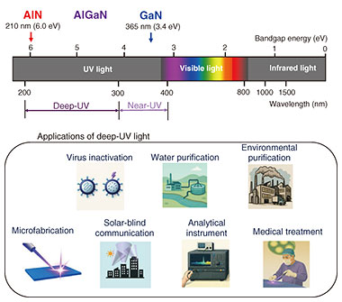
1. Potential applications of deep-ultraviolet light sourcesDeep-ultraviolet (UV) light sources with wavelengths of 200–300 nm are attracting increasing attention for various applications, as shown in Fig. 1. Deep-UV light lies in the wavelength range where nucleic acids, such as DNA (deoxyribonucleic acid) and RNA (ribonucleic acid), are strongly absorbed. Exposure to deep-UV radiation induces photochemical reactions in nucleobases, leading to inactivating bacteria and viruses by impairing their ability to grow and infect hosts. Therefore, deep-UV light is highly effective for applications where hygiene is critical, such as water treatment, environmental purification, and infection control in healthcare facilities and public spaces. Deep-UV light below 280 nm is also important for solar-blind optical communication because background noise remains extremely low even in outdoor environments, enabling stable optical communication. Such solar-blind optical communication is expected to be used in sensor networks for disaster prevention and infrastructure monitoring as well as in short-range communication requiring high confidentiality.
Mercury lamps and excimer lasers have traditionally been used as deep-UV light sources. However, there are several limitations to these sources, including large size, high power consumption, short lifetime, and environmental impact, which have motivated researchers to search for alternative technologies. In this context, nitride semiconductor laser diodes are considered promising candidates for next-generation deep-UV light sources because of their compact size, high efficiency, and long lifetime. Compared with light-emitting diodes (LEDs) that rely on spontaneous emission*1, laser diodes exhibit higher directivity and higher output power and can generate coherent light*2 within a narrower wavelength range. Among nitride semiconductors, gallium nitride (GaN) has a bandgap energy of 3.4 eV, corresponding to a near-UV wavelength of 365 nm, whereas aluminum nitride (AlN) has a larger bandgap energy of 6.0 eV, corresponding to a deep-UV wavelength of 210 nm, as shown in Fig. 1. Aluminum gallium nitride (AlGaN) alloys enable the emission wavelength to be controlled over a wide range by adjusting the composition. In particular, AlN-based materials, including AlGaN with a high Al composition, need to be used to enable light emission in the deep-UV wavelength region below 300 nm. NTT has focused on the potential of AlN as a semiconductor material from an early stage and has researched both materials and devices with the aim of pioneering the use of UV light in semiconductor technologies. In 2006, we successfully demonstrated the world’s first deep-UV AlN LED operating at a wavelength as short as 210 nm, showing the potential of AlN-based semiconductors for deep-UV light-emitting devices [1, 2]. In this article, we summarize the current technical challenges associated with practically implementing deep-UV laser diodes and introduce our latest research results.
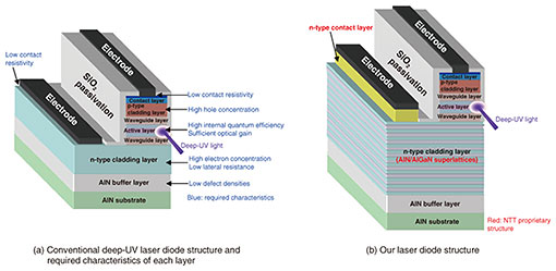
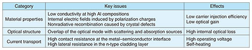
2. Research trends and technical challenges of deep-UV laser diodesDeep-UV semiconductor lasers present significant technical challenges and had long been considered difficult to put into practical use. Nevertheless, since the 2000s, steady progress has been made in understanding the physical properties of AlN, developing high-quality AlN substrates, and advancing AlGaN epitaxial growth and doping technologies. As a result of these advances, laser oscillation in the deep-UV wavelength range (271.8 and 298 nm) has recently been reported [3, 4]. As the emission wavelength becomes shorter, however, the threshold current required for laser oscillation increases, and self-heating caused by increased series resistance becomes more pronounced. In particular, as the wavelength approaches the UV-C region (wavelengths below 280 nm), material properties, optical structure, and current transport become strongly interdependent, reducing the degrees of freedom in device design. Therefore, the multiple technical challenges associated with practically implementing deep-UV laser diodes need to be comprehensively understood. Figure 2(a) shows the main requirements for each layer of an AlN-based deep-UV laser diode and Table 1 summarizes the key issues associated with deep-UV laser diodes from the viewpoints of material properties, optical structure, and current transport. These issues are discussed in the following sections.
For shortening the emission wavelength of AlN-based deep-UV laser diodes, AlGaN with a high Al composition is indispensable. However, as the Al composition increases, constraints arising from the material properties become more pronounced. Typical issues include reduced p-type conductivity, decreased radiative recombination due to internal electric fields caused by polarization charges*3, and increased non-radiative recombination associated with crystal defects such as dislocations and point defects. In p-type AlGaN, the ionization energy of magnesium (Mg) acceptors increases as Al composition increases, which reduces the ionization rate, thus lowering the hole concentration. Similarly, in n-type AlGaN, the ionization rate of silicon (Si) donors decreases as the Al composition increases, resulting in electron concentration reducing. Such decreases in carrier concentration in both the p- and n-type layers limit carrier supply to the active layer and reduce the carrier injection efficiency of the laser diode. From the viewpoint of optical structure, the refractive index difference in the waveguide structure for optical confinement in AlN-based deep-UV laser diodes can, in principle, be controlled by adjusting the composition of the AlGaN layers. However, the composition cannot be varied largely because of constraints related to crystal quality and electrical characteristics at the laser oscillation wavelength. For deep-UV laser diodes operating in the 280-nm wavelength band, the optical confinement factor can reach only a few percent, which is insufficient. Because the optical mode profile is difficult to control, it is easily affected by scattering and absorption caused by donor and acceptor impurities doped in the cladding layers. Thus, internal optical loss increases, leading to threshold current increasing and laser efficiency decreasing. Therefore, in AlN-based laser diodes, it is important to not only ensure optical confinement but also design the optical structure from the viewpoint of suppressing optical loss. Current transport is strongly affected by device structure as well as material properties. In laser diodes with a mesa structure*4, the electrode configuration and current path significantly affect electrical losses. On the n-type side of AlN-based deep-UV laser diodes, the mesa structure causes current to flow laterally in the n-type cladding layer, and this lateral current flow increases the series resistance. Because the lateral resistance is inversely proportional to the effective cross-sectional area of the current path, the thickness of the n-type cladding layer and design of the current path are important factors. In addition, the contact resistance of the electrode depends on the interface characteristics between the metal and the semiconductor. Therefore, issues related to current transport are closely associated with the device structure, including contact resistance.
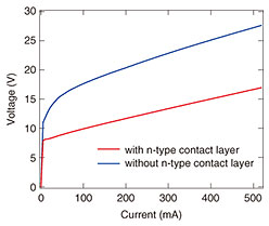
3. Deep-UV laser diodes developed by NTTTo address these issues, NTT has been researching and developing deep-UV laser diodes while comprehensively considering material properties, optical structures, and current transport. We focus on current transport, particularly recent developments in n-type AlGaN contact layers. 3.1 Overview of the device structureFigure 2(b) shows the schematic structure of the AlN-based deep-UV laser diode fabricated for this study. The device structure is epitaxially grown on a low-defect-density AlN substrate through an AlN buffer layer, ensuring high crystal quality. The light-emitting layer consists of AlGaN multiple quantum wells, and the AlGaN optical waveguide layers and cladding layers are arranged above and below the active region to achieve deep-UV emission and optical confinement. On the p-type side, an AlGaN cladding layer and GaN contact layer are formed. On the n-type side, an approximately 3-μm-thick cladding layer composed of Si-doped AlN/AlGaN superlattices is used. This superlattice structure enables the cladding layer to be thicker than conventional n-type cladding layers composed of an AlGaN layer, thus reducing the lateral resistance of the device while maintaining optical confinement [5]. A Si-doped compositionally graded AlGaN layer, in which the Al composition is gradually reduced, is introduced as a unique approach for forming an n-type contact layer in the electrode formation region on the surface of the n-type cladding layer, thereby reducing the contact resistance with the electrode. The laser cavity is formed by cleaving the AlN substrate along the crystal orientation to form mirror facets. The details of the NTT-developed n-type contact layer mentioned above are described below. In conventional AlN-based deep-UV laser diodes, as shown in Fig. 2(a), an electrode is formed directly on the surface of an n-type AlGaN cladding layer with a high Al composition. In this configuration, a large potential barrier forms at the interface between the electrode and n-type cladding layer, which inhibits electron injection from the electrode into the cladding layer and makes a low-resistance ohmic contact*5 difficult to achieve. In our structure, however, a Si-doped compositionally graded AlGaN layer is introduced between the electrode and n-type cladding layer as an n-type contact layer, with the Al composition gradually decreasing toward the electrode, as shown in Fig. 2(b). This enables the electrode to form an interface with AlGaN having a lower Al composition, thus reducing the potential barrier at the interface and facilitating the injection of electrons from the electrode into the n-type cladding layer. This structure also uses a high Si-doping concentration to ensure a high electron concentration, while confining the heavily doped region to the contact layer to minimize its impact on optical properties and crystal quality. This approach enables the resistance of n-type ohmic contacts to be reduced in the deep-UV region by simultaneously optimizing the material composition and doping profile. 3.2 Operating voltage of the laser diodesFigure 3 shows the current–voltage characteristics of deep-UV laser diodes with the n-type contact layer (Fig. 2(b)) and those of conventional laser diodes without the n-type contact layer (Fig. 2(a)). Laser diodes with the n-type contact layer exhibit a lower operating voltage under the same current condition, indicating a lower series resistance. This improvement is attributed to the introduction of the n-type contact layer, which reduces the potential barrier between the electrode and n-type cladding layer and lowers the contact resistance. In devices without an n-type contact layer, however, the resistance associated with the non-ohmic (Schottky) contact at the electrode/semiconductor interface leads to operating voltage increasing. These results indicate that the formation of the n-type contact layer effectively suppresses the increase in operating voltage caused by non-ohmic contact and contributes to reducing the power consumption of the device.
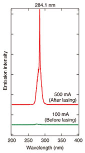
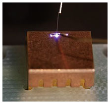
3.3 Emission characteristics of the laser diodeFigure 4 shows the emission spectra of the laser diode with the n-type contact layer fabricated for this study, measured at room temperature under pulsed current injection. As the injection current increases, emissions peak in the deep-UV region. At low injection currents, a broad spectrum dominated by spontaneous emission is observed. At higher injection currents, emissions sharply peak around 284.1 nm; a specific spectral component rapidly increases in intensity, and the spectral linewidth becomes significantly narrower. This behavior indicates that optical gain in the resonator increases, and stimulated emission*6 becomes dominant. Figure 5 shows a photograph of the deep-UV laser diode during operation. Light clearly emits from the laser diode facet. These results indicate that introducing the n-type contact layer improves electron injection efficiency, and that the reduction in operating voltage shown in Fig. 3 is also reflected in the emission characteristics. The results also indicate that the n-type contact layer needs to be optimized for improving the lasing characteristics of deep-UV laser diodes.
4. Future developmentsTo improve the performance of deep-UV laser diodes and promote their practical application, it will be important to not only further optimize the design of electrode interfaces and current paths but also improve carrier injection efficiency into the light-emitting layer and reduce internal optical losses. In deep-UV laser diodes, hole injection efficiency tends to decrease because of the high ionization energy of Mg acceptors in high-Al-content AlGaN. Internal optical losses caused by crystal defects and doped layers increase the threshold current and reduce laser efficiency. Therefore, in addition to conventional Mg doping, material and structural designs for improving hole injection characteristics will be important, including doping methods using polarization charges and carrier control using superlattice structures [6]. Optimizing the quantum-well and barrier-layer structures is considered to effectively improve carrier confinement and achieve high-efficiency emission in the light-emitting layer. A structural design is also needed that reduces internal optical losses caused by optical modes overlapping with scattering and absorption centers, and defects need to be reduced by improving crystal growth and process technologies. Through this series of research and development, the performance of deep-UV laser diodes is expected to improve, leading to broader practical deployment and expanded application fields for deep-UV light sources. References
|
||||||||||||||||||||||||||