|
|||||||||||||||||||
|
|
|||||||||||||||||||
       |
Feature Articles: Forefront Research on Ultrawide-bandgap Semiconductors Vol. 24, No. 6, pp. 54–59, June 2026. https://doi.org/10.53829/ntr202606fa7 Diamond Semiconductors for Spintronic Device ApplicationsAbstractDiamond is a promising platform material for next-generation spintronic device applications due to its outstanding semiconductor and spin properties. The injection of spin-polarized carriers from a ferromagnetic metal into a diamond semiconductor through a tunnel barrier is a key technique for diamond spintronic devices. A Schottky barrier formed at a ferromagnetic metal/diamond interface is a candidate for such a tunnel barrier. We explain the carrier transport mechanism in ferromagnetic permalloy/p-type boron-doped diamond Schottky barrier diodes toward spintronic device applications. Keywords: diamond, Schottky barrier diode, trap-assisted tunneling
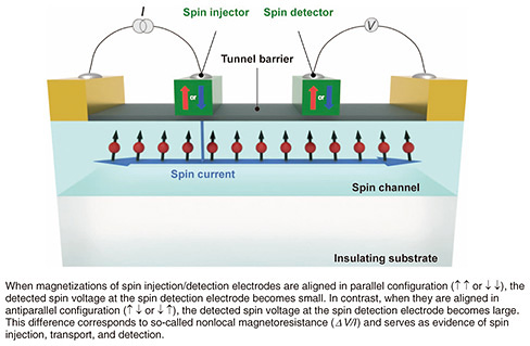
1. Advantages of diamond semiconductors for spintronicsDiamond is widely known as the king of gemstones, and its brilliance has fascinated humanity for centuries. In addition to its attractiveness as a gemstone, diamond also possesses outstanding semiconductor properties, such as high bulk carrier mobilities (4500 and 3800 cm2 V−1 s−1 for electrons and holes, respectively), a high breakdown electric field (> 10 MV cm−1), low dielectric constant (5.7), and high saturation velocities (2.5 × 10⁷ and 1.4 × 107 cm s−1 for electrons and holes, respectively). It has been reported that phosphorus and boron (B) impurities act as donor and acceptor for diamond, respectively. The Baliga and Johnson figures of merit*1 of diamond semiconductors surpass those of industrially mature wide-bandgap semiconductors, such as silicon carbide and gallium nitride. For these reasons, diamond has attracted considerable attention as a platform material for next-generation high-power and high-frequency device applications. Diamond is also a promising platform material for next-generation spintronic device applications. Spin, the intrinsic angular momentum of a particle, is the origin of magnetism, and spintronics, a term combining spin and electronics, is a research field that searches for new spin-related functionalities that are difficult to achieve with conventional charge-based devices. Since spin is a non-conserved quantity that is lost over time and during transport, it is difficult to handle spins in the same way as charges. Compared with other semiconductors, diamond has great potential to preserve spin information for a longer time because it has fewer spin decoherence sources, such as weak spin-orbit interactions and low nuclear spin density. In fact, the diamond nitrogen-vacancy (NV) center hosts a single spin with a millisecond-order spin coherence time even at room temperature, which is among the longest in solid-state materials. Due to this long spin-coherence time, quantum sensors and quantum networks based on diamond NV centers have been extensively studied. Generating spin-polarized carrier flow (spin currents) in diamond may enable manipulation of the spin states of localized NV centers via spin currents [1]. Diamond is expected to have the longest spin diffusion length*2 among semiconductors, enabling interactions between itinerant and localized spins at room temperature. To achieve such new functionalities in diamond, it is essential to understand the underlying spin-related physics in diamond, including the spin diffusion length. However, electrical spin injection into diamond has not yet been demonstrated. Nonlocal spin-valve structures are often used for injecting and detecting spin currents in semiconductors [2]. Figure 1 illustrates the basic structure of a lateral spin-valve device, which consists of ferromagnetic electrodes for spin injection/detection and a spin channel. Inserting a tunnel barrier between a ferromagnetic metal and a semiconductor is generally essential for enhancing spin injection efficiency by controlling the number of carriers tunneling through the barrier, in other words, by controlling the interface resistance [3]. To address this requirement, we focus on using a Schottky barrier*3 formed at the interface between a ferromagnetic permalloy (Py) and a p-type B-doped diamond as a tunnel barrier, where Py is an alloy consisting of 80% nickel and 20% iron. We reveal the carrier transport mechanisms in Py/p-type B-doped diamond Schottky barrier diodes (SBDs) toward electrical spin injection into diamond [4].
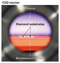
2. Microwave plasma CVD growth of p-type B-doped diamond semiconductorsAmong the crystal growth methods for synthetic diamond, microwave plasma chemical vapor deposition (CVD) is suitable for growing p-type B-doped diamond semiconductors with precisely controlled B concentrations. We have established crystal growth techniques for producing high-quality B-doped diamond films on diamond (001) substrates using a microwave plasma CVD system. To eliminate unintended impurity gases in the CVD reactor, such as water vapor and molecular oxygen, from the gas phase, the pressure under idle conditions is maintained below approximately 1.0 × 10⁻⁷ Torr (approximately one 7.6-billionth of atmospheric pressure). At the beginning of diamond growth, molecular hydrogen, methane, and trimethylboron are introduced into the CVD reactor as source gases. During diamond growth, the pressure is maintained at approximately 25 Torr, and plasma is generated on the diamond substrates by injecting microwaves with a frequency of 2.45 GHz and maximum output power of 1.5 kW (Fig. 2). This plasma decomposes the source gases into radicals. When these radicals are supplied to the surface of a diamond substrate heated to 800–1000°C, only sp3-bonded carbon (C) atoms grow selectively on the substrate, and some of the C atoms are replaced with B atoms, resulting in the formation of a p-type B-doped diamond semiconductor film on the diamond substrate.
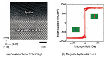
3. Py/p-type B-doped diamond SBDsPermalloy film was deposited on p-type B-doped diamond semiconductor film by electron-beam evaporation to form ferromagnetic Schottky electrodes. Figure 3(a) shows a cross-sectional transmission electron microscope (TEM) image of the interface region. The B-doped diamond film shows a single-crystalline structure with clear lattice images, reflecting the periodic arrangement of sp3-bonded C atoms. The interface is atomically abrupt without the formation of an interfacial reaction layer that would degrade spin injection efficiency. From the magnetic hysteresis curve of the Py film (Fig. 3(b)), we confirmed that the Py film has the typical ferromagnetic properties of Py even on the B-doped diamond film. When a sufficiently large positive magnetic field is applied, the magnetization saturates at about 820 emu/cm3. This indicates that the Py film has a large magnetic moment due to the alignment of spins in the same direction. On the other hand, when the polarity of the magnetic field changes from positive to negative, the magnetization rapidly switches from positive to negative.
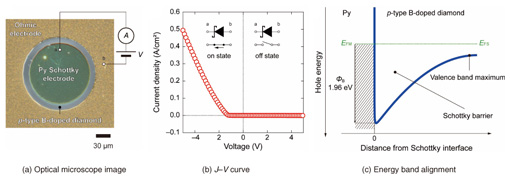
The Py/B-doped diamond stacking structure was then processed into SBDs, as shown in Fig. 4(a). Figure 4(b) shows the current density–voltage (J–V) characteristics of a representative SBD with a B concentration of 8.0 × 1017 cm−3 (corresponding to approximately one B atom per 220,000 C atoms). Under forward-bias conditions (V < 0), J rapidly increases (on state), while under reverse-bias conditions (V > 0), J is almost zero (off state). These results indicate that this SBD exhibits typical rectifying behavior. The Schottky barrier height (ΦB) was also estimated to be about 1.96 eV from the capacitance–voltage characteristics. These results indicate that a Schottky barrier is formed at the Py/B-doped diamond interface, as illustrated in the energy band diagram of Fig. 4(c) [4].
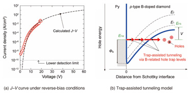
4. Carrier transport mechanism under reverse-bias conditionsWe next investigated the carrier transport mechanism under reverse-bias conditions (V > 0), which corresponds to the direction in which spin is injected from Py film into p-type B-doped diamond semiconductor film. When a high reverse-bias voltage is applied to the same SBD shown in Fig. 4(b), J gradually increases, as shown in Fig. 5(a). To investigate the origin of the carrier transport under reverse-bias conditions, we developed a trap-assisted tunneling (TAT) model that incorporates B-related hole trap levels in the depletion region, as illustrated in Fig. 5(b), on the basis of the energy band diagram shown in Fig. 4(c). For the B-related hole trap levels, we assumed a B acceptor level (E1 = EV – 0.37 eV) and B dimer level (E2 = EV – 1.21 eV) [5]. The J–V characteristics under reverse-bias conditions calculated using the TAT model are shown with the black dashed line in Fig. 5(a) and are in good agreement with the experimental results. We therefore found, for the first time, that tunneling via B-related hole trap levels is the dominant carrier transport mechanism in Py/B-doped diamond SBDs. These results suggest that a Schottky barrier formed at the Py/B-doped diamond interface can be used as a tunnel barrier for spin injection.
5. SummaryAs part of our initiatives toward spintronic devices using diamond semiconductors, we investigated the carrier transport mechanism under reverse-bias conditions in Py/p-type B-doped diamond SBDs. We will fabricate the obtained structure into a spin-valve device to demonstrate spin injection, clarifying the underlying spin-related physics in diamond. References
|
||||||||||||||||||