|
|||||||||
|
|
|||||||||
|
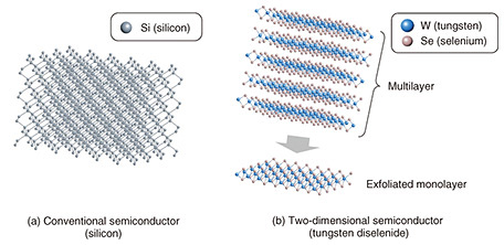
Rising Researchers Vol. 24, No. 6, pp. 8–13, June 2026. https://doi.org/10.53829/ntr202606ri1  Pioneering Valley Physics with Two-dimensional SemiconductorsAbstractCurrent information and communication technologies form the foundation of people’s lives and economic activities, and much of the information processing involved in those activities is carried out by electrons. Research has focused on properties of electrons other than electric charge, and with the advent of two-dimensional semiconductors, a new degree of freedom called “valleys” has attracted attention. Strongly linked to the polarization of light, valleys have the potential to lead to the creation of new means of information processing and optical functions. We interviewed Haruki Sanada, a distinguished researcher who is taking on the challenge of identifying and controlling valleys in two-dimensional semiconductors. Keywords: two-dimensional semiconductor, electron, valleytronics  Research on valleytronics—Exploring ultrathin semiconductors—What are two-dimensional semiconductors? Inside the personal computers and smartphones we use every day, semiconductor materials, such as silicon and gallium arsenide, are used in components for information processing and wireless communication. These semiconductors form crystals in which atoms are bonded regularly in three dimensions by covalent bonds (Fig. 1(a)). In contrast, a type of material that has recently attracted considerable attention has a two-dimensional layered structure, in which atoms are bonded only within the plane. Among these materials, those with semiconductor properties are called “two-dimensional semiconductors” (Fig. 1(b)). Two-dimensional semiconductors typically consist of many layers stacked on top of each other; however, like layers of a pastry, they can be easily separated. Theoretically, it had long been predicted that reducing these layered materials to an ultimate single layer would produce new physical phenomena not seen in three-dimensional crystals. However, isolating a single layer proved difficult. This situation was dramatically changed in 2004 when a method for exfoliating a single layer of graphene from layered graphite was reported by researchers who later won the Nobel Prize. The discovery of this method triggered rapid progress in research on two-dimensional materials, including two-dimensional semiconductors.
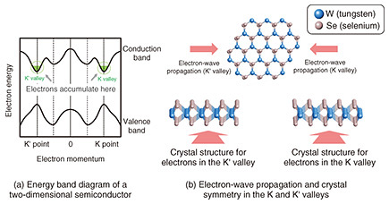
—Why are valleys in the electronic band structure of two-dimensional semiconductors attracting attention? Understanding valleys requires some knowledge of energy band diagrams, which are used in solid-state physics. An energy band diagram shows how the kinetic energy of electrons changes with momentum, and its shape depends on the material. “Valleys” refer to the minima that appear in this energy band diagram, and electrons tend to accumulate in the valleys. In such a diagram of two-dimensional semiconductors, as shown in Fig. 2(a), two deep valleys (called K valley and K' valley) appear, and these valleys give rise to physical phenomena that differ from those of conventional semiconductors. The direction in which the phase of the electron wave propagates in the K and K' valleys corresponds to a specific direction in the crystal (Fig. 2(b), top). The bottom diagram of Fig. 2(b) compares how the crystal structure appears differently to electrons in the K and K' valleys when viewed along the direction of electron-wave propagation. Even within the same crystal, electrons experience different atomic environments depending on the direction of electron-wave propagation. For this reason, even at the same energy, electrons in the K and K' valleys are considered to be in different states. In other words, the valleys provide a new and promising degree of freedom.
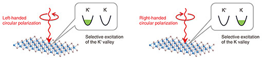
Another well-known degree of freedom of electrons is spin. Spin is an intrinsic property of electrons in quantum mechanics. It can take two states—often described as clockwise and counterclockwise, or simply as up and down—and research aimed at using this property is known as spintronics. Valleys can be considered a degree of freedom, similar to spin. The research field that aims to use this property is called “valleytronics.” In two-dimensional semiconductors, physical properties depend on which of the two valleys an electron occupies. If we can identify and control these valleys, this can lead to new insights into fundamental physics and future applications in information processing. —How can spins and valleys be used in information processing? In conventional information processing, digital information is represented by “0” and “1,” typically based on the presence or absence of electrical charge. In contrast, the basic idea in spintronics and valleytronics is to use spin and valley degrees of freedom to encode information as “0” and “1.” However, spin and valley are not widely used in current semiconductor devices because these states are usually randomly distributed, making them difficult to control and use reliably as information. Despite this difficulty, spin and valley continue to attract many researchers because they are quantum-mechanical states and possess the property of superposition. That is, they can not only take on one of two binary states but also exist in multiple states simultaneously. This property is expected to enable new ways of handling information and new functions beyond conventional binary (“0” and “1”)-based information processing. —Would you tell us about your research on the interaction between valleys and light? One important feature of two-dimensional semiconductors is that valleys are strongly linked to the circular polarization of light. As shown in Fig. 3, by using right- and left-handed circular polarization, we can selectively generate and observe specific valley states. This ability to directly manipulate valleys via light is a major feature not found in conventional semiconductors.
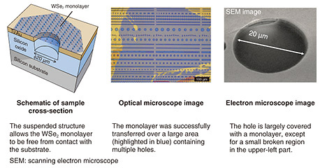
The coupling between valleys and light also enables optical extraction of valley-related information and control of valleys through the polarization and propagation direction of light. By taking advantage of this property, we are working to develop new optical functionalities and explore novel physical phenomena on the basis of the interaction between valleys and light. Visualizing and controlling valleys using light—Would you tell us about techniques for visualizing invisible degrees of freedom using light? The experimental technology for observing and controlling the valley degree of freedom via light was originally developed by our research team after nearly 10 years of studying electron spin [1]. Electron spin is an invisible degree of freedom, so without a way to capture its state, we cannot easily understand or control it. To address this challenge, we first established a method for visualizing electron spin optically. This unique method uses the magneto-optical effect to directly determine how spin is generated and how it evolves over time and space. We also devised a new way to control spin without using an external magnetic field [2, 3]. We are currently extending these optical methods to two-dimensional semiconductors and applying them to research on the observation and control of valleys as a new degree of freedom. —Would you tell us about your recent research on suspended monolayers? This research was carried out with key contributions from Giacomo Mariani, an Italian researcher in our research group. By covering tiny holes drilled in a substrate with a monolayer of two-dimensional semiconductor, we created a suspended monolayer, which is not in contact with the surrounding material. Our aim was to elucidate the intrinsic behavior of valleys while minimizing the impact of the external environment. As shown in the left image of Fig. 4, thin films of titanium (Ti) and gold (Au) are formed on a silicon substrate, and holes of various sizes (e.g., 10-μm diameter and 0.8-μm depth) are fabricated through the metal films into the substrate. The substrate is then covered with a monolayer of the two-dimensional semiconductor tungsten diselenide (WSe2) [4]. Since monolayers are fragile, it is difficult to fabricate large-area suspended monolayers, but we achieved this through repeated trial and error in a cleanroom. Optical and electron microscope images of a suspended monolayer are shown in the center and right panels of Fig. 4, respectively.
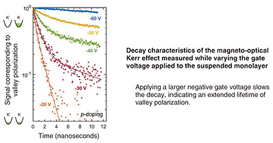
The fabricated suspended monolayer was placed in a vacuum at liquid helium temperatures (−269°C), and the valley polarization was measured using an optical method based on the magneto-optical effect. This enabled us to investigate physical processes such as valley formation and relaxation, significantly advancing our understanding of valley physics, which had previously been understood only indirectly. We experimentally investigated how long valley polarization could be sustained under different voltages applied to the suspended monolayer. The results indicate that the polarization disappears quickly at −20 V, whereas it persists longer at −60 V (Fig. 5). These findings open up new possibilities for new device applications using valley degrees of freedom.
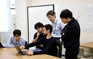
—Would you tell us about the future developments and applications of this research? From the perspective of fundamental science, we are working in both competition and collaboration with research institutions worldwide to unravel the physics of valleys in two-dimensional semiconductors. Investigating phenomena never seen before will not only contribute to scientific advancement but also drive the development of entirely new technologies and concepts. Two-dimensional semiconductors had mainly been studied at basic level; however, as conventional semiconductor miniaturization approaches its limits, research toward practical applications of two-dimensional semiconductors has begun to emerge. The high-speed and controllability of valleys make them promising for photonic technologies in the Innovative Optical and Wireless Network (IOWN). In the future, valleytronics could be integrated with NTT’s in-chip optical communication and related technologies. Our research is closely aligned with the goals of IOWN, as it focuses on physical properties strongly linked to light. Since valleytronics is an active field worldwide, we are keen to disseminate our unique research findings and become a group that naturally attracts researchers interested in collaboration. We hope to expand our capabilities through communication and collaboration with other researchers and aim to take a leading role in a new research field that fuses valleys and photonics. —Would you tell us what inspired you to start this research and what you consider important in your work? My initial motivation for pursuing this research field stemmed from the term “spintronics,” which I first encountered during a university lecture. I was fascinated by the idea that semiconductors have a largely untapped property called spin that can be used to create new functionalities. Subsequently, I joined the professor’s research group, where I studied spin dynamics in semiconductors using an optical approach during my doctoral studies. Around that time, NTT researchers in this field were also publishing groundbreaking results in rapid succession. I felt that their work was at the forefront of the field and closely aligned with my research interests. This was a major reason I joined NTT. What I value most in research is the attitude of always verifying our ideas through experiments, leading to new questions. Although I sometimes encounter unexpected problems, I feel that the real thrill of research comes from solving them step by step. I also believe that one of the roles of a researcher is to present the results clearly and logically, explain how they contribute to society, and communicate those findings effectively. Our group conducts research with young researchers and students from Japan and abroad. For example, we currently host several interns from European universities. While these collaborations certainly help nurture the next generation, I find great value in sharing the excitement of science with colleagues from diverse backgrounds. I believe that through these experiences, we can play a meaningful role in advancing scientific research in Japan and worldwide. —Would you tell us about NTT Basic Research Laboratories, where you work? NTT Basic Research Laboratories aims to create new principles and concepts that transcend the limitations of network technology, develop fundamental technologies leading to future innovations, and acquire universal knowledge that will contribute to NTT’s business. Our research activities focus on three core areas: Multidisciplinary Materials Science, Advanced Applied Physical Science, and Quantum Science and Technology, and are driven by the curiosity of our researchers. With leading researchers in each field, we provide an environment where researchers can inspire one another. My research group primarily conducts experimental research, and we work in the lab almost every day. Nevertheless, some members flexibly incorporate remote work depending on their research phase and personal circumstances. We also host international researchers and students from our collaborating institutions, creating a lively and interactive research environment (Photo 1).
—Finally, what message would you like to share with researchers and students? Due to the impact of the COVID-19 pandemic, many young people have had limited opportunities to gain hands-on experience or have face-to-face discussions. Now that things have returned to normal, I hope that students and researchers will actively take on new challenges that they could not pursue before. Communication is an essential part of research. Building connections with others and sharing the excitement of science will contribute to the future of science. I’d also like to encourage researchers who are interested in two-dimensional semiconductors and valleytronics—as well as those who aspire to pursue basic research and explore phenomena that no one has ever seen before—to join NTT Basic Research Laboratories. Together, we can open new doors and push the boundaries of our understanding of physical phenomena. References
■Interviewee profileHaruki Sanada received a B.E., M.E., and Ph.D. in electrical engineering from Tohoku University, Miyagi, in 2001, 2002, and 2005. He joined NTT Basic Research Laboratories in 2005 and started his research on the optical and spin properties of low-dimensional semiconductor nanostructures. He was a visiting researcher at Chalmers University of Technology, Sweden, in 2015. In 2019, he took on responsibilities in administrative and personnel management at NTT Basic Research Laboratories. In 2022, he was appointed Group Leader of the Quantum Optical Devices Research Group. He received the RIEC Award from the Research Institute of Electrical Communication, Tohoku University in 2014, and the Young Scientists’ Prize of the Commendation for Science and Technology by the Minister of Education, Culture, Sports, Science and Technology of Japan in 2016. He is a member of the Japan Society of Applied Physics. |
|||||||||