|
|||||||||||||||||||||||||
|
|
|||||||||||||||||||||||||
        |
Front-line Researchers  Pioneering One-of-a-kind Materials Synthesis to Create and Understand High-temperature SuperconductorsAbstractSuperconductivity—the complete disappearance of electrical resistance in materials when they are cooled below a critical temperature (Tc)—has fascinated scientists for more than a century. Raising Tc remains one of the greatest scientific challenges of the 21st century. Hideki Yamamoto, a senior distinguished researcher at NTT Basic Research Laboratories, is tackling this challenge by creating novel superconductors through NTT’s world-leading thin-film synthesis technologies. Together with his colleagues, he is pursuing the discovery of unprecedented high-temperature superconductors and uncovering the fundamental mechanisms behind their remarkable properties. Their work could pave the way toward a carbon-neutral future. Keywords: superconductor, thin-film synthesis, electron impact emission spectroscopy
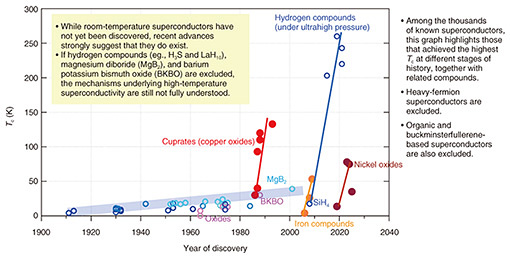
Toward room-temperature superconductors: Exploring complex oxides to complex nitrides through thin-film synthesis—Would you tell us about your current research? For many years, we have been pursuing three goals by using proprietary equipment developed in house at NTT: growing high-quality thin films of known complex oxides and nitrides, creating entirely new superconductors, and uncovering the physics behind them. We have synthesized and discovered six new families of superconductors and two new families of magnetic materials, classified according to their crystal structures. These new superconductors include entirely new materials enabled by the design of artificial superlattice structures [1, 2]. Superconductivity is the phenomenon in which a material loses electrical resistance and expels magnetic fields (the Meissner effect) when cooled below its superconducting transition temperature (Tc). Materials that exhibit this phenomenon are known as superconductors. Although thousands of superconductors have been discovered, a room-temperature superconductor remains elusive. Superconductivity was first discovered in 1911 by the Dutch physicist Heike Kamerlingh Onnes (1853–1926). Using helium that he had successfully liquefied, he found that the electrical resistance of mercury suddenly dropped to zero at the extremely low temperature of approximately 4.2 K (Kelvin)—or minus 269°C. Although various superconductors were subsequently discovered, progress in raising Tc was slow. A major breakthrough came in 1986 with the discovery of cuprate superconductors, triggering an intensive worldwide search that pushed Tc above 100 K within just a few years. Such materials are known as high-temperature superconductors. Some of these materials become superconducting when cooled using inexpensive liquid nitrogen rather than liquid helium, and practical applications, such as power cables and high-magnetic-field magnets, are underway. In 2019, a hydrogen-rich compound was reported to exhibit superconductivity at a temperature much closer to room temperature (i.e., minus 25°C) than previously achieved, albeit at ultrahigh pressures of two million atmospheres. This remarkable result strongly suggests that room-temperature superconductors may indeed exist. Attention has recently focused on nickel-oxide superconductors, which possess crystal structures similar to those of cuprates, and are expected to exhibit high Tc (Fig. 1).
However, several papers claiming the discovery of room-temperature superconductivity were found to contain fabricated data and were subsequently retracted. If a material exhibiting room-temperature superconductivity at ambient pressure were discovered, it could eliminate electrical resistance, hence power loss, in power transmission lines and circuit wiring, making a major contribution toward achieving carbon neutrality. With such enormous potential, it is no surprise that the global race to discover new superconductors has become increasingly intense. While the excitement surrounding possible breakthroughs is understandable, every claim must ultimately stand up to rigorous scientific scrutiny. Although conventional low-temperature superconductivity is well explained by BCS theory*1, the mechanism of high-temperature superconductivity remains one of the greatest unsolved problems in condensed-matter physics. As someone engaged in the search for and synthesis of new superconductors with high Tc, I’m also striving to elucidate the mechanism of high-temperature superconductivity and establish design principles for creating new superconducting materials. Among our most recent achievements, the emergence of superconductivity in thin-film ruthenium oxide (RuO2) is particularly noteworthy. It is known that RuO2 is not superconducting in its bulk*2 form; superconductivity has been observed only in thin films. It had generally been assumed that the superconductivity originated from the strain imposed on the thin film by the substrate. However, my colleague Senior Researcher Yoshiharu Krockenberger grew RuO2 thin films with various crystallographic orientations and found, through detailed structural analysis, that superconductivity emerges from a new crystal phase distinct from that of the bulk material [3]. This finding is particularly important because it demonstrates that even materials with the same chemical composition can exhibit entirely different physical properties when their crystal structures differ. As part of our search for new superconductors, we have also been working on the synthesis of complex nitrides since around 2021. One reason for focusing on nitrides is that they generally have a stronger covalent character than oxides; in other words, their constituent atoms have a greater tendency to bond by sharing electrons. I believe that, as in cuprate superconductors, materials featuring strongly covalent structural units, such as two-dimensional covalent networks, are more likely to exhibit high Tc. This leads me to hope that complex nitrides could eventually yield superconductors with Tc exceeding those of the cuprates. Although nitrogen makes up approximately 80% of the atmosphere, with most of the remainder consisting of oxygen, far fewer nitrides than oxides have been synthesized. Nitrides can therefore be regarded as a largely unexplored class of materials. I find this particularly fascinating because nitrides are inherently difficult to form—as illustrated by the fact that many metals do not undergo nitridation simply upon exposure to air. My colleagues, Researcher Kosuke Takiguchi and Senior Researcher Yoshiharu Krockenberger, have succeeded in synthesizing a completely new type of complex-nitride thin film. Using this material as a starting point, our immediate goal is to create or discover a nitride superconductor with a Tc exceeding the current record of approximately 25 K [4]. This research is underpinned by NTT’s world-leading thin-film synthesis technology. Using the well-known superconductor titanium nitride (TiN) as an example, we recently prepared single-crystal superconducting thin films, the crystalline quality of which even surpasses that of bulk crystals, and clarified their physical properties [5]. We are thus pursuing a unique approach to superconductivity research that combines the inheritance and further refinement of our unparalleled technology with the creation of ultrahigh-quality thin films, elucidation of their physical properties, and search for previously undiscovered superconductors.
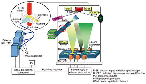
From thin-film synthesis to a new view of high-temperature superconductivity—What were the biggest challenges along the way? The first challenge was technological. The synthesis of both oxides and nitrides requires precise, simultaneous control of the deposition rates of all the constituent elements in molecular beam epitaxy (MBE), the thin-film growth technique we adopted. In MBE, atomic or molecular beams are directed onto a single-crystal substrate, where they react to form the desired material. Over many years, NTT has developed a world-leading MBE platform and accumulated extensive expertise, particularly in the synthesis of complex oxides and nitrides (Fig. 2).
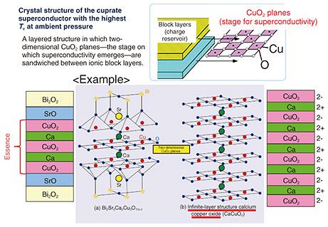
For more than three decades, NTT has relied on a key technology—electron impact emission spectroscopy (EIES)—to precisely control the supply of elements constituting the thin film. In EIES, electrons emitted from a filament are accelerated and collide with atoms traveling through the vacuum from each source material. The light emitted by an atom is then analyzed to monitor the flux of each element. In a sense, it is like identifying the ingredients of a firework from the colors it produces. By using EIES, it is possible to control the supply rate of each element constituting the thin film with atomic-level precision. However, EIES equipment has frequently faced threats to its continued existence because manufacturers either discontinued the product or were acquired by other companies. Ultimately, commercial production of EIES systems came to an end in 2025. Fortunately, we had anticipated this situation and had spent nearly five years developing our own proprietary system at NTT. I’m relieved that we have preserved this unique technology and ensured that it can be passed on to the next generation of researchers. The next challenge was nitride synthesis. As I mentioned earlier, nitrides are extremely difficult to synthesize, and producing new nitride materials sometimes requires temperatures exceeding 1000°C. To achieve this, we adopted a laser-heating system manufactured by a Polish company. At first glance, it might seem that simply purchasing and installing the system would solve the problem. In reality, however, we had to develop techniques for operating at much higher synthesis temperatures while maintaining the performance of the rest of the thin-film growth system and establish a highly reproducible synthesis process. We also devoted considerable effort to finding efficient ways to promote nitridation in an ultrahigh-vacuum deposition environment. Among the proprietary technologies we have developed are innovative plasma-source designs for efficiently generating atomic nitrogen, together with methods for systematically controlling nitridation strength. —You’ve overcome major challenges in developing the equipment needed for your research. What drew you to thin films in the first place? The prevailing view is that the best way to study physical properties of a material is to use large, high-quality, bulk single crystals, because they are generally regarded as providing the most reliable results. However, if there are sound scientific reasons thin films can better reveal the intrinsic properties of a material, then thin films may actually offer deeper insights into its true nature. That is also why I believe NTT’s world-class thin-film synthesis technology is far too valuable to let fade away. Working on thin films has given me more than just new materials, it has also changed the way I think about high-temperature superconductivity. A major focus of our research is to understand the mechanism of high-temperature superconductivity, and it was precisely our work on thin films that led me to develop my own ideas about why high-temperature superconductors share common features in their crystal structures and chemical bonding, as well as what kind of materials should be synthesized to achieve high Tc. For oxide materials, for example, thin films have a much higher surface-area-to-volume ratio and much shorter oxygen diffusion distance than their bulk counterparts. As a result, they enabled us to observe how physical properties can change dramatically with even subtle variations in oxygen content or arrangement. We also realized that, while covalent bonds are generally regarded as strong, in cuprate superconductors, the copper–oxygen (Cu–O) bonds within the CuO2 planes responsible for superconductivity are surprisingly weak (Fig. 3).
A widely discussed mechanism for high-temperature superconductivity is the spin-fluctuation mechanism, in which fluctuations of antiferromagnetic order mediate an attractive interaction between electrons, enabling them to form Cooper pairs. My own perspective is somewhat different. I believe that high-temperature superconductivity may ultimately be explained as an extension of BCS theory. Without going into technical details, in materials such as cuprate superconductors, quasi-two-dimensional superconducting layers with relatively weak covalent bonds are sandwiched between ionically bonded charge-reservoir layers. I hypothesize that, under such conditions, unusually strong electron-lattice interactions—beyond those considered in conventional BCS theory—might emerge, giving rise to high-temperature superconductivity through a charge-fluctuation mechanism. Some researchers have argued that the two-dimensional nature of the CuO2 planes is the key to high-temperature superconductivity. If increased two-dimensionality alone were the decisive factor, one might expect superconductivity to be enhanced as the films are made thinner. Yet no such systematic enhancement has been observed. This can only be demonstrated through highly reproducible experiments using exceptionally high-quality thin films. Testing theories and hypotheses requires more than technical skills; it also demands scientific intuition and a certain aesthetic sense, qualities that can only be cultivated through sophisticated experimentation. In any case, my perspective is still held by only a minority of researchers, and one of my biggest challenges is convincing others of its validity. After many years of thin-film research, I now feel that the path toward obtaining conclusive evidence is finally coming into view. I’ve also come to understand why such experiments could not have been carried out before; the necessary experimental tools simply did not exist. —How are you working to demonstrate your perspective? I’m investigating the behavior of electrons in materials using techniques such as photoelectron spectroscopy and X-ray absorption spectroscopy. As part of this work, we have begun experiments at NanoTerasu, a state-of-the-art synchrotron-radiation facility that began operation in April 2024 located adjacent to Tohoku University in Aoba Ward, Sendai, Japan. Synchrotron radiation is produced when electrons traveling at nearly the speed of light are forced to move around a circular orbit, emitting an intense beam of light tangential to their orbit. Japan’s best-known synchrotron facility, SPring-8, is renowned for its high-intensity hard X-rays (wavelengths shorter than 0.1 nm). NanoTerasu, by contrast, is optimized for soft X-rays (0.1–10 nm), making it particularly well suited for probing electronic states and chemical bonding at the nanoscale, revealing electronic structures and chemical bonding that were previously inaccessible. One unique aspect of NanoTerasu is that it was built through a public–private–regional partnership. As one of the coalition members, NTT contributed to the facility’s construction and is allocated priority beamtime for experiments. By taking advantage of its exceptionally bright, high-quality light, we can now carry out experiments in a fraction of the time previously required. For example, we can analyze the electronic states of more than a dozen samples in just two days. Looking ahead, I also hope that our work will contribute to making NanoTerasu an even more powerful facility for materials research. From 2015 until March 2024, I served as head of our research department. Since stepping down from that role, I have been back in active research for the past two years. Although it has taken some time to regain my research instincts, I truly enjoy being back in the laboratory. Going forward, I hope to continue pursuing the synthesis and discovery of new superconductors while working to elucidate the mechanisms of high-temperature superconductivity by combining world-leading thin-film samples with advanced spectroscopic techniques. Breakthroughs come from diverse expertise—What message would you like to share with those who will follow in your footsteps? Breakthroughs sometimes emerge only after years of patient collaboration, eventually leading to publications in leading journals [6–8]. One such breakthrough came from combining unique, high-quality samples prepared at NTT with advanced spectroscopic techniques, including experiments conducted at major overseas synchrotron-radiation facilities, through close collaboration with outstanding research partners. Establishing international collaborations often requires considerable time and effort, but I would encourage young researchers to embrace such opportunities whenever they have the potential to produce truly unique results. After all, international research experience and collaboration are essential for conducting world-leading research. However, we have increasingly been reminded that research does not exist in a vacuum. With prices in many Western countries already far higher than in Japan—and the weak yen further reducing our purchasing power—stagnant research budgets have become an even greater challenge. Geopolitical tensions and visa restrictions have also made it increasingly difficult for some researchers to participate in international conferences and collaborations. Despite these challenges, we live in an era in which truly original discoveries, built on years of accumulated expertise, can be shared instantly with the world through the Internet. I therefore encourage young researchers to devote themselves wholeheartedly to pursuing research that only they can accomplish. I also encourage young researchers to develop expertise across multiple fields. A good example is Researcher Kosuke Takiguchi, who had joined NTT only two years earlier when, in 2023, he played a central role in growing high-quality TiN thin films and investigating their physical properties. While refining his experimental skills, he also conducted collaborative research at the Japan Advanced Institute of Science and Technology, where he developed expertise in computational materials science and conducted electronic-structure calculations for thin films with crystal structures different from those of their bulk counterparts [5]. His achievements perfectly illustrate that breakthroughs come from diverse expertise. One final thought. I encourage you to publish important findings regardless of the journal’s profile, especially when your experimental results or interpretations challenge established theories. One example from my own research concerns the electronic phase diagram—a map illustrating how a material’s electronic state changes with temperature or carrier doping*3—which is central to understanding high-temperature superconductivity. Work of this kind may not attract much attention at first, but it can suddenly become important as new discoveries are made by others or as advances in measurement technology reveal new facts, even decades later. Measurement technology has advanced remarkably over the past three decades. Today, we can see and measure things in ways that were simply unimaginable when I began my research career. I hope the next generation of researchers will make the most of these extraordinary opportunities and never hesitate to pursue ideas that they truly believe in.
References
■Interviewee profileHideki Yamamoto received a B.S., M.S., and Ph.D. in chemistry from the University of Tokyo in 1990, 1992, and 1995. He joined NTT in 1995, and his principal research fields are thin-film growth, surface science, and condensed-matter physics, with a particular focus on superconductivity. He was a visiting scholar at the Geballe Laboratory for Advanced Materials, Stanford University, USA (2004–2005). At NTT Basic Research Laboratories, he served as executive manager of the Research Planning Section (2013–2015) and the Multidisciplinary Materials Design and Science Laboratory (2015–2024). He received the 2nd Young Scientist Presentation Award (1997) from the Japan Society of Applied Physics (JSAP) and the 20th Superconductivity Science and Technology Award (2016) from the Forum of Superconductivity Science and Technology, the Society of Non-traditional Technology. He is a member of JSAP, the Physical Society of Japan, the Japan Society of Vacuum and Surface Science, the American Physical Society, and the Materials Research Society. |
||||||||||||||||||||||||