|
|||||||||||||||||||||||||
|
|
|||||||||||||||||||||||||
       |
Vol. 5, No. 9, pp. 20–25, Sept. 2007. https://doi.org/10.53829/ntr200709sp3 System for Measuring the Phase Transition Temperature of KTa1−xNbxO3 Using Scanning Nonlinear Dielectric MicroscopyAbstractWe have developed a system for measuring the paraelectric-to-ferroelectric phase transition temperatureTC using scanning nonlinear dielectric microscopy (SNDM). We developed a probe for samples with a huge dielectric constant and demonstrated that theTC of potassium tantalate niobate (KTa1−xNbxO3, KTN) crystal can be measured locally using SNDM with this probe. The TC measurement precision (standard deviation) is 0.09°C. This corresponds to a composition (Nb concentration x) resolution of 1.4 × 10⁻⁴, which is difficult to achieve with other element analyzers. Moreover, by measuring TC while changing the position, we demonstrated that we can measure the spatial distribution of the TC of the KTN crystal. To reduce the time required for the operator to measure the TC distribution of the KTN crystal, we developed software for fully automated operation. 
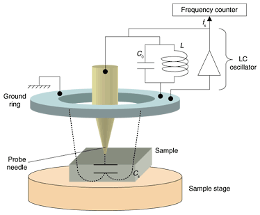
1. IntroductionPotassium tantalate niobate (KTa1−xNbxO3, KTN) is a ferroelectric material and its dielectric constant and quadratic electro-optic (EO) constant (Kerr constant) are maximum around the paraelectric-to-ferroelectric phase transition temperature (TC) [1]. These values are huge, so KTN is expected to reduce both the volume and driving voltage of EO devices, such as optical beam deflectors [2] and modulators [3]. In KTN, TC can be adjusted by changing the composition, i.e., the Ta/Nb ratio [1]. TC increases linearly with the amount of Nb (x) [4]. However, if there is a spatial change in the Ta/Nb ratio in a crystal, which may be induced by changes in the growth condition during crystal growth, TC changes spatially, and the dielectric constant ε and the Kerr constant s change spatially at a given temperature. If a crystal’s spatial distributions of ε and s are large (i.e., the crystal is highly inhomogeneous), it is difficult to guarantee the characteristics of an EO device manufactured from that crystal. Therefore, to guarantee the characteristics of a KTN device, it is necessary to evaluate the uniformity of a crystal’s TC before the device is manufactured. However, if TC has to be estimated with a precision of 0.1°C, the composition should be estimated with a precision of 1.5 × 10⁻⁴ [4]. This is difficult to achieve with conventional element analyzers, such as an electron probe microanalyzer (EPMA). In this paper, we describe the system for measuring the TC of KTN that we developed. First, we review scanning nonlinear dielectric microscopy (SNDM) and describe the probe we developed for samples having a huge dielectric constant. Then, we describe our demonstration that the TC of KTN crystal can be measured locally using SNDM with our probe. Experimental results for TC measurement precision and the spatial distribution of the TC of the KTN crystal are also presented. Finally, we introduce the software developed to reduce the time taken for the operator to measure the TC distribution of a KTN crystal. 2. Scanning nonlinear dielectric microscopy (SNDM)2.1 Principle of SNDMScanning nonlinear dielectric microscopy (SNDM) has been developed to measure the local dielectric constant under a probe needle with high spatial resolution [5], [6]. Moreover, non-destructive measurement is possible, so a crystal that has been evaluated using SNDM can be used for manufacturing devices. A schematic diagram of SNDM is shown in Fig. 1. SNDM uses an LC (inductance and capacitance) oscillator with a probe needle. When the probe needle is far away from the sample, the resonant frequency f0 is ,
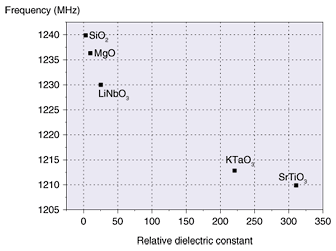
To check this, we measured the resonant frequency of several dielectric materials. The relationship between fS and the dielectric constant at room temperature is shown in Fig. 2. This figure clearly indicates that the larger the dielectric constant, the lower fS. Accordingly, when fS is measured as a function of temperature, the local TC can be obtained as the temperature that gives the lowest fS. Moreover, the spatial distribution of TC can be measured by changing the point touched by the probe.
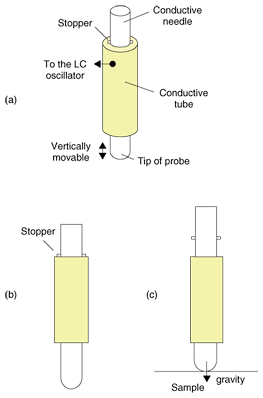
2.2 Probe for keeping contact force constantIn crystals with a huge dielectric constant, such as KTN, fS depends strongly on the contact force that the probe needle exerts on the sample. The reason for this is as follows: when the probe needle is in point contact with a sample having a huge dielectric constant, the electric field is concentrated in a very small area just under the tip of the probe needle [7], and fS depends on the capacitance of that very small area. When the contact force is stronger, the contact area is larger due to deformation, and fS depends on the capacitance of the larger area and is lower; namely, fS depends on both the dielectric constant and the contact force. In the work described here, we developed a probe that keeps the contact force constant during the measurement of TC. A schematic diagram of the probe is shown in Fig. 3(a). The probe consists of a conductive tube and a conductive needle that can move up and down in the tube, which has a stopper to prevent the needle from falling out. When the tip of the probe is not in contact with a sample, the needle is held by the stopper, as shown in Fig. 3(b). On the other hand, when the tip is in contact, the sample pushes the needle upwards, as shown in Fig. 3(c). With this design, the contact force is equal to the force of gravity acting on the needle and can be kept constant.
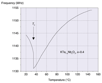
3. Experimental results3.1 Measurement of TC of KTNThe resonant frequency fS is plotted as a function of temperature T in Fig. 4 when the probe needle (Au-coated, tip radius: 500 µm) came into contact with a KTN single crystal (6 × 5 × 0.5 mm3, x ≈ 0.4). We estimated TC to be about 35°C because domains appeared or disappeared at this temperature. The fS was about 1214 MHz when the probe needle was kept far away from the sample; namely, CS = 0. We used a Peltier device and a controller to sweep the temperature and we collected data during the cooling phase. The sweep rate was not constant, but the average rate was about 0.3°C/s. As shown in the figure, fS was minimum at around 35°C. This indicates that SNDM can measure the TC of KTN.
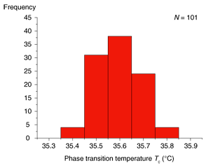
3.2 TC measurement precisionWe evaluated the precision of this method. We performed the TC measurement N times, where N = 101. A histogram of TC is shown in Fig. 5. Here, for TC, we used the temperature at which dfS/dT was the smallest because it changes drastically around TC, as shown in Fig. 4. This large change is induced by an abrupt change in the dielectric constant. The mean value of TC,
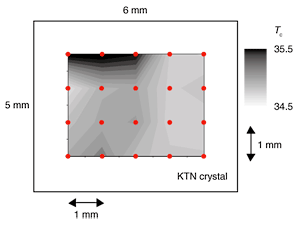
3.3 Spatial distribution of TCNext, we evaluated the TC distribution of the crystal. We measured TC at 20 (= 5 × 4) points with a spacing of 1 mm. The distribution is shown in Fig. 6. For this crystal, TC is higher in the top left of the figure. The maximum and minimum TC values were 35.37 and 34.7°C, respectively. Here, TC = 35.37°C corresponds to x = 0.4091 and 34.7°C to x = 0.4081, where x is the amount of Nb. Therefore, the variation in TC in this crystal was 0.67°C, which corresponds to a variation in composition of about 0.001 using the above empirical equation [4].
4. Measurement systemTo reduce the time required for the operator to evaluate the TC distribution of the KTN crystal, we automated the measurement and data processing. A window of the software we developed is shown in Fig. 7. After the measurement condition (measurement spacing and number of points etc.) has been assigned and the sample has been set, the measurement is finished in a fully automated manner. Moreover, to eliminate manual data processing after the measurement, the software detects TC by a differential calculation, as discussed in section 3.2 and records it.
5. ConclusionWe described our system for measuring the phase transition temperature TC of KTN using SNDM and a newly developed probe designed to keep the contact force constant during the temperature sweep. The precision (standard deviation) is 0.09°C, which corresponds to a composition resolution of 1.4 × 10⁻⁴. By measuring TC while changing the position, we demonstrated that we could measure the TC distribution of the KTN crystal. We also developed software capable of measuring the TC distribution of the KTN crystal in a fully automated manner. This measurement system will enable the uniformity of KTN crystals to be evaluated, so it will be possible to guarantee the characteristics of KTN devices made from KTN crystals. 6. AcknowledgmentsWe thank Professor Yasuo Cho of Tohoku University for fruitful discussions about SNDM. References
|
||||||||||||||||||||||||