 |
|||||||||||||||||||||||||||
|
|
|||||||||||||||||||||||||||
       |
Selected Papers: MEMS Device Technologies Vol. 5, No. 10, pp. 17–23, Oct. 2007. https://doi.org/10.53829/ntr200710sp3 STP Technology for Sealing
|
||||||||||||||||||||||||||

| † | NTT Microsystem Integration Laboratories Atsugi-shi, 243-0198 Japan Email: nsato@aecl.ntt.co.jp |
|---|
1. Introduction
The mechanically movable parts of microelectromechanical systems (MEMS) devices must be protected from dust and moisture to ensure that they move properly in practical environments. We have been developing seamless integration technology in order to stack MEMS devices ranging in size from 10 mm to 1 mm on LSIs (large-scale integrated circuits) [1]. An example of a three-dimensional MEMS structure comprising of an upper electrode and a lower electrode on a silicon substrate is shown in Fig. 1. When a bias voltage is applied between the two electrodes, the upper electrode is coupled to the lower one by electrostatic force. A cavity provides the free space for the upper electrode to move. The challenge has been how to seal the cavity to protect the movable parts while preventing the sealant from flowing into the cavity.
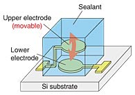
Fig. 1. MEMS device with a movable part.
A common sealing technique for LSIs is to cover a bare LSI chip with plastic resin. Only connectors protrude from the mold. This technique works because LSI chips do not have cavities. Anodic bonding of silicon and glass substrates has been used to protect MEMS structures. The drawback is that the bonding process requires high temperature and high voltage, which can damage MEMS devices.
We have been investigating fabrication processes for MEMS devices, in particular, the critical processes for film formation and patterning. Our work has led to the development of technology using spin-coating film transfer and hot-pressing (STP), which is suitable for sealing MEMS structures that contain cavities.
2. Concept of STP
In the fields of LSIs and MEMS, spin-coating and vapor deposition have been widely used for film formation and have been applied directly to wafers. The underlying principle of these techniques is deposition, and it is impossible to prevent dielectric materials from depositing inside cavities. The underlying principle of STP, on the other hand, is transfer using a base film as a temporary substrate, and this enables us to form dielectrics over cavities.
In STP, the concept is to transfer dielectrics from a base film to a wafer as a substrate [2]. This is achieved through the procedure outlined in Fig. 2. First, a varnish of dielectric material is spin-coated onto the base film to a thickness of 1 to 10 µm. In the spin-coating step, the varnish is spread into a thin film by centrifugal force to completely cover the base film (Fig. 2(a)). Next, the dielectric on the base film is hot pressed against a wafer with hollow structures in a vacuum (Fig. 2(b)). In this step, the dielectric varnish dries and hardens. Then, the base film is peeled off from the wafer in air at room temperature (Fig. 2(c)). Finally, the dielectric on the wafer is thermally cured. As a result, the hollows are sealed without the cavities being filled in.
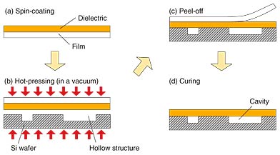
Fig. 2. Concept of the STP process.
3. Transfer apparatus and viscosity control for STP
To implement the principle and perform the procedure described above, we devised an STP transfer apparatus [3] because the most critical step in Fig. 2 is the hot-pressing step, in which the shape of the dielectric is determined. A photograph of the transfer apparatus with its chamber open is shown in Fig. 3. The apparatus features a tension ring and hot-pressing heaters in the vacuum chamber.
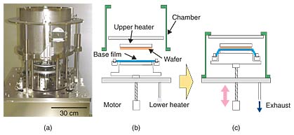
Fig. 3. Transfer apparatus for STP. (a) Photograph of the apparatus and schematicdiagrams of its operation (b) before and (c) during hot pressing.
What happens inside the transfer apparatus is explained with the help of schematic images in Figs. 3(b) and (c). First, a wafer is attached face down to the upper heater. Next, a dielectric spin-coated onto a base film is set on the lower heater facing the wafer surface. The base film, which is transparent, after spin-coating is shown in Fig. 4(a). Then, the chamber is closed and evacuated. In the vacuum, the lower heater is raised using a motor. As the lower heater rises, the base film is uniformly stretched with the tension ring to remove wrinkles. After further elevation, the dielectric makes contact with the wafer surface. The position of the lower heater is then kept constant to apply a press force of preset magnitude (Fig. 3(c)). After that, the lower heater is lowered to its initial position. Then, the chamber is purged with N2 gas to atmospheric pressure. The dielectric and base film attached to the wafer are taken out of the chamber. Finally, the base film is peeled off from the wafer. Thus, the dielectric is transferred from the base film to the wafer as shown in Fig. 4(b).
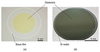
Fig. 4. Photographs of (a) the base film after spin-coating and (b) Si wafer after the base film was peeled off.
Along with the transfer apparatus, we have developed a method for controlling the shape of the transferred dielectrics [4]. It is necessary to control the shape of the dielectric film as shown in Fig. 5(a) for planarization and sealing. The intermediate state is not favorable due to air pockets and bubbles. We speculated that the key factors determining the shapes of the dielectrics are the material's viscosity and the press force during the hot-pressing step. Since the dielectric material's viscosity can be changed by drying through heating in the vacuum chamber, viscosity control is suitable for STP. To clarify the effects of viscosity on the shape, we devised a simple analytical model that uses the solution of the two-dimensional Poiseuille flow under the condition that the dielectric is incompressible and its amount is constant. The calculated relationship between the material viscosity and press force is shown in Fig. 5(b). Planarization and gap-filling are possible when a large press force is applied to a soft, low-viscosity dielectric. On the other hand, we can seal hollow patterns when a small press force is applied to a hard, high-viscosity dielectric.
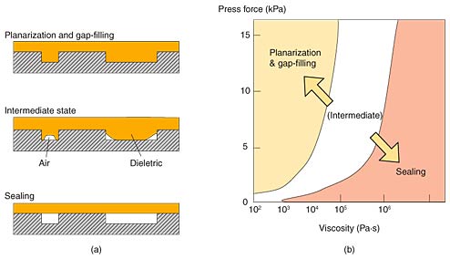
Fig. 5. (a) Schematic cross-sectional views of the shapes of the dielectrics after STP and (b) the calculated relationship between viscosity and press force.
4. Results for sealing characteristics
We performed film-formation experiments using the transfer apparatus and the control method described above. Images taken with a scanning electron microscope (SEM) after STP are shown in Fig. 6. We successfully sealed hollow structures 20 µm deep with a 20-µm-thick dielectric (Fig. 6(a)). The dielectric material did not flow into the cavities. On the other hand, we achieved planarization of the hollow patterns by controlling the dielectric's viscosity and the press force (Fig. 6(b)). These results confirm that the transfer apparatus and viscosity-control method are effective for STP.
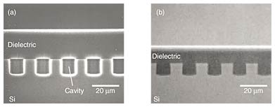
Fig. 6. Cross-sectional SEM images of (a) sealing and (b) planarization.
Next, we clarified the sealing characteristics by determining the relationship between the width of the hollow pattern and the thickness of the dielectric. The experimental results indicate that there is a region where sealing is successful, as shown in Fig. 7. Cross-sectional SEM images corresponding to typical conditions A to D are also shown in Fig. 7. These results confirm that STP is an enabling technology applicable for widths and thicknesses of around 10 µm, for which conventional techniques cannot be used.
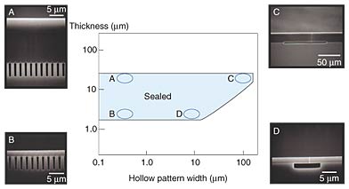
Fig. 7. Sealing characteristics for various hollow patterns.
5. Application to MEMS devices
Here, we explain a MEMS fingerprint sensor as an example of the application of STP. We fabricated a sensor LSI chip, as shown in Fig. 8(a) [5], [6]. When a finger touches the chip, the chip detects the fingerprint pattern. A magnified SEM image of the sensor surface is shown in Fig. 8(b). Square pixels with protrusions are arrayed in a 256 × 224 matrix with a pitch of 50 µm. Each pixel corresponds to a dot in the fingerprint image, and 57,344 pixels in total compose a fingerprint image. A cross-sectional SEM image of a pixel is shown in Fig. 8(c).
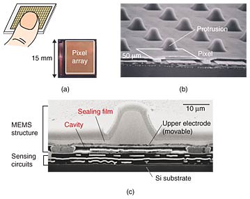
Fig. 8. (a) Schematic image and a chip photograph. SEM images of (b) the surface and (c) cross-section of a pixel of the MEMS fingerprint sensor.
When a finger touches the sensor surface, a pattern of ridges, each several hundred micrometers wide, pushes down the protrusions in several pixels. Since there is a 1-µm cavity between the upper and lower electrodes of the pixel in Fig. 8(c), the upper electrode is movable. The downward movement of the protrusion deforms the upper electrode, which increases the capacitance between the two electrodes. The underlying sensing circuits detect the slight increase in capacitance of several femtofarads and output the amplified value.
In such capacitive sensors, the capacitance between the electrodes is drastically affected by moisture in practical environments. Therefore, the cavities have to be sealed to ensure that the capacitance is not affected by the external environment. We sealed the cavities with a 1.5-µm-thick sealing film by using STP, as shown in Fig. 8(c), and achieved stable operation of the MEMS fingerprint sensor.
6. Conclusion
We described spin-coating film transfer and hot pressing (STP) and a transfer apparatus and viscosity-control method suitable for it. Film-formation experiments showed that film shape can be controlled for planarization and sealing. We also clarified the cavity sealing characteristics by investigating how the sealing depends on pattern size and dielectric thickness. STP was applied to the fabrication of MEMS fingerprint sensors. The successful sealing of the cavities protected the capacitive electrodes from the external environment, which contributed to the stable operation of the sensors. Therefore, STP is an enabling technology for various kinds of MEMS devices.
References
| [1] | H. Ishii, H. Morimura, and J. Kodate, “MEMS Device Technology for Ubiquitous Services,” NTT Technical Review, Vol. 5, No. 10, 2007. https://www.ntt-review.jp/archive/ntttechnical.php?contents=ntr200710sp1.html |
|---|---|
| [2] | K. Machida, H. Kyuragi, H. Akiya, K. Imai, A. Tounai, and A. Nakashima, “Novel global planarization technology for interlayer dielectrics using spin on glass film transfer and hot pressing,” J. Vac. Sci. Technol. B, Vol. 16, No. 3, pp. 1093–1097, 1998. |
| [3] | N. Sato, K. Machida, K. Kudou, M. Yano, and H. Kyuragi, “Advanced Transfer System for Spin Coating Film Transfer and Hot-pressing in Planarization Technology,” J. Vac. Sci. Technol. B, Vol. 20, No. 3, pp. 797–801, 2002. |
| [4] | N. Sato, K. Machida, M. Yano, K. Kudou, and H. Kyuragi, “Advanced Spin Coating Film Transfer and Hot-pressing Process for Global Planarization with Dielectric-material-viscosity Control,” Jpn. J. Appl. Phys., Vol. 41, No. 4B, pp. 2367–2373, 2002. |
| [5] | N. Sato, S. Shigematsu, H. Morimura, M. Yano, K. Kudou, T. Kamei, and K. Machida, “Novel Surface Structure and Its Fabrication Process for MEMS Fingerprint Sensor,” IEEE Trans. Electron Devices, Vol. 52, No. 5, pp. 1026–1032, 2005. |
| [6] | N. Sato, H. Ishii, S. Shigematsu, H. Morimura, T. Kamei, K. Kudou, M. Yano, K. Machida, and H. Kyuragi, “A Sealing Technique for Stacking MEMS on LSI Using Spin-coating Film Transfer and Hot Pressing,” Jpn. J. Appl. Phys., Vol. 42, No. 4B, pp. 2462–2467, 2003. |
 |
|
|---|---|
 |
|
 |
|
 |
|
 |
|
 |
|