|
|||||||||||||||||||||||||||
|
|
|||||||||||||||||||||||||||
       |
Selected Papers: MEMS Device Technologies Vol. 5, No. 10, pp. 24–29, Oct. 2007. https://doi.org/10.53829/ntr200710sp4 Integrated RF-MEMS Technology for Reconfigurable RF TransceiversAbstractThis paper describes a novel structure and fabrication process for integrated RF-MEMS (radio frequency microelectromechanical systems) technology. This technology features a multilayer structure and an encapsulation process for the integration and protection of RF MEMS devices. Various types of encapsulated RF-MEMS devices, such as switches and varactors, were fabricated on the same substrate simultaneously. Experimental results indicate that this technology is promising for the development of small low-power reconfigurable RF transceivers. 
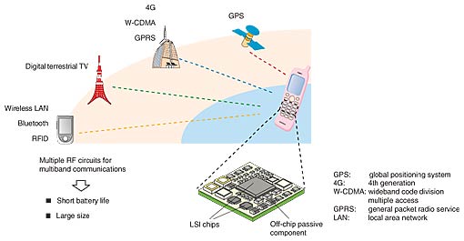
1. IntroductionVarious types of wireless communication services are provided around the world through mobile phone networks, wireless local area networks, and RFID (radio frequency identification) systems. With the globalization and diversification of wireless communications, many wireless standards have been established over a wide range of frequencies to provide such services. To make various services available everywhere, we need small low-power RF transceivers capable of multiband operation. As shown in Fig. 1, currently available RF transceivers consist of several LSI chips and numerous off-chip passive components. Increasing the number of available communication bands will increase the number of components and make RF transceivers larger. It will also increase power consumption and shorten battery life. Reconfigurable RF circuits, which can change circuit configurations according to the wireless standards to be used, would enable multiband operation without increasing the size and power consumption. However, the performance of conventional switches and tunable passive devices needed for such reconfiguration is insufficient. RF-MEMS (radio frequency microelectromechanical systems) technology is attracting interest for the fabrication of high-performance RF devices for reconfigurable RF circuits [1], and several types of RF-MEMS devices, such as switches, variable capacitors (varactors), inductors and filters, have been developed. One problem with conventional RF MEMS devices is that they have been developed as discrete components, and using many RF-MEMS devices increases the size of RF transceivers. Another problem is related to packaging. RF-MEMS devices have movable parts that can be easily damaged or destroyed during packaging processes, such as wafer dicing.
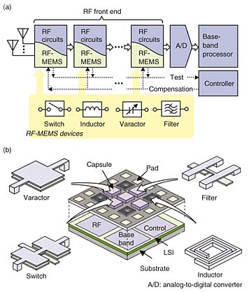
To solve these problems, we have developed integrated RF-MEMS technology for the integration and protection of RF-MEMS devices. For integration, an adaptable multilayer structure and its fabrication process enable fabrication of various types of RF-MEMS devices on the same substrate. For protection, a wafer-level encapsulation process forms small thin capsules to protect RF-MEMS devices. This paper first explains the concept of our technology. Next, it describes the structure and fabrication process for the devices. Finally, it presents experimental results. 2. Integrated RF MEMS technologyThe aim of integrated RF-MEMS technology is to integrate various types of RF-MEMS devices and RF circuits to develop single-chip reconfigurable RF transceivers [2]. The circuit diagram of an RF receiver using RF-MEMS devices is shown in Fig. 2(a). The RF receiver is composed of antennas, RF front-end circuits, an analog-to-digital converter, a baseband processor, and a control circuit. RF-MEMS devices, such as switches, filters, varactors, and inductors, are integrated with the RF front-end circuits. These devices provide reconfigurability and enable multiband operation. For example, switches having low insertion loss and high isolation can reconfigure a circuit according to the communication band, and varactors with wide-range tunability provide wideband oscillators. The integration of RF-MEMS devices and a control circuit also enables on-chip testing and compensation of the devices. This reduces the variation in device characteristics and improves productivity while eliminating the need for extra LSI (large-scale integration) chips.
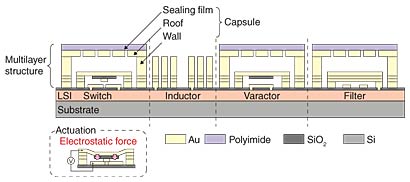
The configuration for integrated RF MEMS technology is conceptually illustrated in Fig. 2(b). Several types of RF-MEMS devices are simultaneously formed on top of an LSI and connected to the circuits. This configuration reduces the volume consumed by discrete packaging of the devices and allows the use of a lot of devices without increasing the number of off-chip components. RF-MEMS devices with movable parts, such as switches, are protected by a device-scale capsule to prevent their destruction during packaging. The protective capsule allows the use of conventional LSI packaging technology. This technology will lead to the fusion of RF-MEMS and circuit technologies and to the development of single-chip reconfigurable RF transceivers. 3. Device structureThe device structure for integrating different types of RF-MEMS devices is illustrated in Fig. 3. The devices are formed in multiple layers and protected by a capsule. The stacking of multiple layers forms various thicknesses and gaps, providing adaptability for integration. Because each layer is fabricated by the same process at the same time, several types of devices can be formed simultaneously.
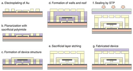
Each capsule is composed of walls, a roof, and a sealing film. The walls and roof are formed at the same time as the devices, and the etching holes in the roof are sealed with thin film by using a selective sealing technique (see section 4). For compatibility with LSI fabrication, the devices use electrostatic actuation. Applying a voltage between electrodes displaces the movable electrode so that it moves towards the fixed electrode. This enables various electromechanical functions, such as signal switching, capacitance tuning, and frequency filtering. The electrostatic actuation can be implemented without using special materials, such as piezoelectric material, which would make it difficult for the process to be compatible with LSI fabrication. The device structure enables the fabrication of integrated, protected RF-MEMS devices on an LSI. 4. Fabrication processThe fabrication process for the device structure is based on seamless integration technology [3]. The process flow for a switch in a capsule is shown in Fig. 4. First, the lower structures of the switch, such as lower interconnections, are formed on the substrate by Au electroplating (Fig. 4(a)). Next, the lower structures are planarized with photosensitive polyimide (Fig. 4(b)). The polyimide is a sacrificial layer and is removed later. Then, other parts of the switch and the capsule are formed by repeating the electroplating and planarization (Figs. 4(c) and (d)). This stacking process simplifies the fabrication of the multilayer structure. At this point, the sacrificial layers are removed by dry ashing through etching holes in the roof (Fig. 4(e)). Finally, the etchings holes are sealed with photosensitive polyimide by transferring the sealing film onto the roof. This film transfer is accomplished by using spin-coating film transfer and hot pressing (STP), a technology that we developed ourselves (Figs. 4(f) and (g)) [4]-[6]. The encapsulation protects the integrated RF-MEMS devices without damaging them.
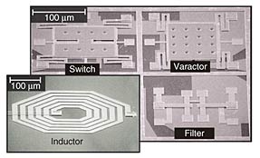
5. Experimental resultsWe fabricated the integrated RF-MEMS devices shown in Fig. 5. The images were taken before encapsulation to show the devices. Different kinds of RF-MEMS devices, such as switches, varactors, inductors, and filters, were fabricated on the same substrate by stacking multiple layers. The devices are about 200 µm × 200 µm in size, and the thicknesses and gaps range from less than 0.5 µm to over 10 µm. The multilayer structure enables this wide range of thicknesses and gaps.
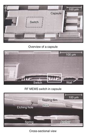
The integrated RF-MEMS devices were encapsulated using STP technology. Figure 6 shows SEM photographs of (a) a capsule covering a switch and (b) the inside of the capsule, where a switch was properly encapsulated. Figure 6(c) shows a magnified view of the beam of the switch and the roof of the capsule. It is clear that the etching holes in the roof were sealed with the film. These images show that the encapsulation of RF-MEMS devices was successful.
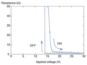
The electrical characteristics of integrated RF-MEMS devices were measured. DC-measurement results for a switch are shown in Fig. 7. A voltage of more than 16 V applied between the top and bottom electrodes activated the switch, and low resistance of 1.5 Ω was obtained. The switch was turned on and off and it operated repeatedly.
These results confirm that different types of RF-MEMS devices with encapsulation can be fabricated on the same substrate. 6. ConclusionWe have developed elemental techniques for integrated RF-MEMS technology. The multilayer structure and its fabrication process enabled us to fabricate different types of RF-MEMS devices on the same plane. An STP-based encapsulation technique has also been developed to protect the devices. Several types of protected RF-MEMS devices were fabricated, and the operation of a switch was demonstrated. These techniques will pave the way for the development of reconfigurable RF transceivers with integrated RF-MEMS devices. References
|
||||||||||||||||||||||||||