|
|||||||||||||||||||||||
|
|
|||||||||||||||||||||||
       |
Selected Papers: MEMS Device Technologies Vol. 5, No. 10, pp. 30–35, Oct. 2007. https://doi.org/10.53829/ntr200710sp5 High-yield Fabrication Methods for MEMS Tilt Mirror Array for Optical SwitchesAbstractWe have developed high-yield fabrication methods for a microelectromechanical systems (MEMS) tilt mirror array having high-aspect-ratio torsion springs and terraced electrodes that enable reliable tilt motion. Experimental results show that the tilt mirror motion is reliable, which makes the mirror array promising for application to 3D MEMS optical switches. 
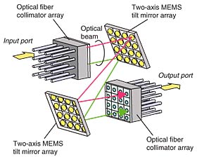
1. IntroductionOptical microelectromechanical systems (MEMS) are promising for many optical components. Three-dimensional (3D) MEMS optical switches are attracting great interest as large-scale all-optical switching fabrics because of their great potential to lower cost, reduce power consumption, and provide compactness and high optical performance. Several MEMS optical switch fabrics have been reported and received with keen interest [1], [2]. The basic configuration of a 3D MEMS optical switch module using free-space optical interconnections is shown in Fig. 1. The module consists of a two-axis MEMS tilt mirror array and an optical fiber collimator array. There is a dedicated mirror for each input and each output port. Optical beams from input ports are collimated by the collimator array and reflected twice by the two-axis MEMS tilt mirror. When the mirrors are tilted two-dimensionally, the optical beam is deflected two-dimensionally as well. Connection between any input port and any output port can be achieved by controlling the tilt angle of each mirror.
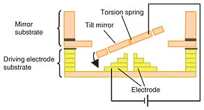
The MEMS mirror array is a key functional component of the 3D MEMS optical switch [3]. The characteristics of the optical switch greatly depend on the characteristics of the mirror array itself, such as flatness and reflectivity. Many types of single-crystal silicon mirrors with good characteristics have been introduced [4]. However, little has been reported about the methods of fabricating mirror arrays. We have developed practical high-yield processes for fabricating MEMS mirror arrays and have used them to build an MEMS tilt mirror array with high-aspect-ratio torsion springs that enable reliable tilt motion. This paper describes the structure of our developed MEMS tilt-mirror array and the fabrication methods. It also presents experimental results for mirror tilt motion that indicate that the mirror array is promising for application to 3D MEMS optical switches. 2. MEMS mirror structureA cross-sectional schematic of the two-axis MEMS tilt mirror is shown in Fig. 2. The MEMS mirror consists of two single-crystal silicon substrates: the mirror substrate and driving electrode substrate. These substrates are processed independently and flip-chip bonded to each other so that an air gap is formed between the mirror and electrodes. The mirror is actuated by electrostatic force generated by applying voltage between the mirror and electrodes. The tilt angle of the mirror is controlled by applying a driving voltage to each electrode.
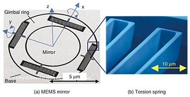
2.1 Mirror substrateSEM photographs of a two-axis MEMS tilt mirror and a torsion spring are shown in Figs. 3(a) and (b), respectively. The MEMS mirror, which is 600 µm in diameter, is supported by a pair of folded torsion springs and connected to a gimbal ring on the x axis. The gimbal ring is connected to the base by another pair of folded torsion springs on the y axis. Consequently, the mirror turns on the x and y axes so that it can steer the optical beam in 3D space. The mirror and the torsion springs are made of single-crystal silicon, which provides highly reliable mirror motion. The torsion springs have a high aspect ratio, which is defined as the ratio of spring thickness to spring width. These high-aspect-ratio springs have a large stiffness in the z direction relative to the torsion direction, which prevents the mirror from being pulled down and contacting the electrodes.
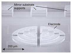
2.2 Driving electrode substrateAn SEM photograph of the four electrodes with 3D terraced structure is shown in Fig. 4. The mirror is actuated by electrostatic force generated by applying voltage to each electrode. The electrostatic force is inversely proportional to the square of the gap between the mirror and the electrode. The 3D terraced electrode structure reduces the gap compared with the conventional flat electrode structure and thereby permits a low driving voltage.
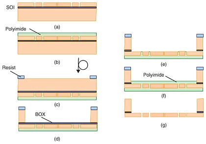
3. Fabrication methods3.1 Mirror electrode substrateThe process flow for the mirror substrate is shown in Fig. 5. First, mirror patterns are formed on a silicon-on-insulator (SOI) wafer by lithography and dry etched (Fig. 5(a)). Polyimide is then spin-coated over the formed mirror (Fig. 5(b)). The patterns for the mirror opening on the reverse bulk-Si side are formed (Fig. 5(c)) and then dry etched using a resist mask. The buried oxide (BOX) works as an etching stopper (Fig. 5(d)). The BOX is removed with hydrofluoric acid (Fig. 6(e)), and then polyimide is spin-coated again on the other side of the coated mirror surface (Fig. 5(f)). The polyimide protects the mirrors against shocks during the dicing step. The protective layer of polyimide is then ashed off by exposing it to oxygen plasma after the dicing process (Fig. 5(g)). Using this dry process to release the mirrors in this final stage prevents the so-called in-process stiction of the mirrors and improves process yield.
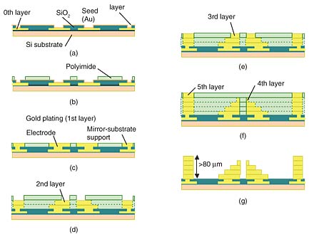
The flatness of the mirror surface affects the optical characteristics of the switch containing the mirror arrays. Both sides of the mirror surface are coated with Au to reduce warpage of the mirror surface and the Au coating on the top surface also ensures good reflectivity. The peak-to-valley difference is 0.05 µm, indicating a very flat mirror surface. 3.2 Driving electrode substrateThe process flow for the driving electrode substrate is shown in Fig. 6. The process begins with thermally oxidized Si wafers. After the formation of the 0th level interconnection, a metal layer of Au/Ti is deposited by evaporation. The Ti layer acts as an adhesive and the Au layer as a seed for successive electroplating (Fig. 6(a)). Then, polyimide is spin-coated and the electrodes and the mirror-substrate supports in the first layer are patterned lithographically (Fig. 6(b)). After the lithography process, Au is electroplated (Fig. 6(c)). In electroplating, the metal's thickness varies with the area to be plated because of the difference in current density on the wafer. Therefore, we designed the areas to be electroplated for each electrode to be as similar as possible in order to obtain a flat surface over the whole wafer after electroplating. For this purpose, we formed the mirror-substrate supports with a solid rectangular structure, as shown in Fig. 4. The flat surface is produced by adjusting the area to be electroplated and controlling the plating time. Repeating the polyimide coating, photolithography, and gold electroplating processes (Figs. 6(b) to 6(e)) yields thick-gold multilevel electrodes embedded in over 80 µm of polyimide (Fig. 6(f)). Finally, the sacrificial layer of polyimide is ashed away by exposure to oxygen plasma (Fig. 6(g)). These processes produce electrodes and mirror-substrate supports that are over 80 µm high, which ensures enough space to tilt the mirror on the electrodes.
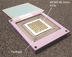
4. MEMS mirror motionA photograph of a packaged MEMS mirror array with mirror substrate flip-chip bonded to the driving electrode substrate is shown in Fig. 7. If there is an alignment error in the bonding process, the centers of the mirror and electrodes will be misaligned, resulting in nonuniformity of the mirror motion characteristics in the tilt direction and crosstalk between the tilt motion around the x and y axes. High alignment accuracy is required to prevent these problems.
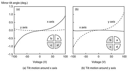
The relationship between the tilt angle of the mirror and applied voltage is shown in Fig. 8. The crosstalk with tilting between rotations around the x and y axes is very small. This confirms the accurate alignment of the mirror substrate and driving electrode substrate, which means that the 3D terraced electrodes can operate the mirror precisely.
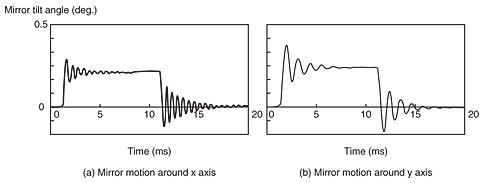
The step responses of the tilt motion around the x and y axes are shown in Fig. 9. The responses coincide with the damped oscillation determined by the designed mirror inertia and torsion spring stiffness.
References
|
||||||||||||||||||||||