|
|||||||||||||||||||||||||||||||||||||||||||||||||
|
|
|||||||||||||||||||||||||||||||||||||||||||||||||
       |
Regular Papers Vol. 8, No. 8, pp. 31–37, Aug. 2010. https://doi.org/10.53829/ntr201008rp1 Direct Actuation of GaAs Membrane Resonator by Scanning ProbeAbstractA method for evaluating the mechanical properties of microresonators and nanoresonators with high spatial resolution is described. Mechanical vibration is directly induced into a circular resonator by voltage applied from a conductive microprobe, and the nanometer-order amplitude of the resonator is simultaneously measured by a scanning probe microscopy system. The resonant properties of 200-nm-thick GaAs circular membranes with a diameter of 14–64 µm were measured and the resonant frequencies were found to range from 0.65 to 5.18 MHz. The minimum detectable amplitude was about 1 nm. The amplitude distributions of the fundamental mode and higher modes were successfully observed with nanometer resolution. 
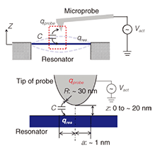
1. IntroductionMicroelectromechanical systems (MEMS) and nanoelectromechanical systems (NEMS) are expected to provide “More than Moore’s Law” devices for future electronics. In MEMS/NEMS, resonant structures are key components for ultralow-mass sensing and single-charge detection [1]–[3]. Optical interferometry and optical deflection techniques, which use laser beams, are standard methods for detecting dynamic mechanical motion with nanometer-order amplitude [4]. However, the spatial resolution of these methods is limited by the diffraction limit of the optical systems. To realize the full potential of MEMS/NEMS, we need to develop a new method for detecting nanometer-order amplitudes with high-spatial resolution. Vibration detection using the microprobe of a scanning probe microscope (SPM) is a promising method for detecting nanovibrations with nanometer-order resolution [5]–[10]. Since the effective contact force in an SPM’s dynamic force mode is small enough compared with the vibration energy of MEMS/NEMS, the resonator’s vibration envelope can be imaged with high-spatial resolution. Vibration detection in various microresonators and nanoresonators, such as single-crystal silicon cantilever devices [5], carbon nanotube beams [6], [7], and graphene membranes [8] has been demonstrated using the SPM-based technique. The key to improving the SPM-based method is a simple actuation method for microresonators and nanoresonators. In previous studies [5]–[8], additional structures or devices were required to actuate the resonators. One of the most effective and easiest ways to actuate them is to use a piezoelectric actuator [5]. However, the cut-off frequency of the piezo-device is limited by its macroscopic size, so it is not suitable for nanomechanical resonators. Another way is to drive the actuation by the Coulomb force from additional electrodes [6], [7]. However, this method requires complex fabrication processes for the additional electrodes, so it is very difficult to put the electrodes near the target structures. To overcome these problems, we tried to get the SPM microprobe itself to play the role of the actuator in order to eliminate the additional actuating devices. The probe actuates the membrane resonator directly, and nanometer-order amplitudes at megahertz-order frequencies can be detected simultaneously [10]. 2. Simultaneous excitation and detection of resonator vibrationIn our method, the vibration of the membrane structure is excited by the voltage applied from the conductive probe of the SPM system, as schematically shown in Fig. 1. The minimum distance between the probe and membrane is almost zero because the probe is controlled in the dynamic force mode. Since the Coulomb force strongly depends on the distance, a smaller SPM probe amplitude is preferable for actuation. The typical amplitude in our experiment was about 20 nm. Because the effective probe force is very small, the vibration of the membrane is not affected by observation using the SPM probe. The minimum detectable vibration amplitude of the membrane is about 1 nm.
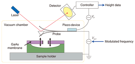
The experimental setup of our measurement system is shown in Fig. 2. The sample was simply set in the vacuum chamber of the SPM system (E-sweep from SII-NT). A probe coated with metal (Rh) having a spring constant of 53 N/m was connected to the function generator supplying actuation voltage (Vact) at a modulated frequency. The height information was monitored by the SPM controller (Nanonavi from SII-NT). Since the feedback speed of the SPM controller is very low compared with the vibration of the membrane, we could observe the envelope of the membrane motion. The typical tip radius of the metal-coated probe was about 30 nm, which is suitable for high-spatial resolution observation of a vibrating membrane. All the experiments discussed in this paper were done in vacuum at room temperature.
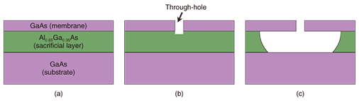
3. Fabrication process of membrane resonatorA 200-nm-thick single-crystal non-doped GaAs epitaxial layer grown on a 1-µm-thick Al0.65Ga0.35As layer was used as the membrane resonator in our experiments (Fig. 3(a)). A small through-hole was fabricated in the top GaAs layer by optical lithography with dry etching or focused ion beam (FIB) direct etching (Fig. 3(b)). The Al0.65Ga0.35As layer was sacrificially etched using diluted HF solution (Fig. 3(c)). Circular membranes with a diameter ranging from about 10 to 100 µm were obtained by this simple fabrication method.
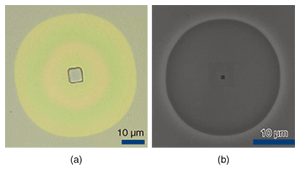
Micrographs of the fabricated membranes are shown in Fig. 4. The membrane with a 65-µm-diameter (a) was fabricated by conventional optical lithography. FIB nano-lithography could fabricate smaller membranes. The 26-µm-diameter membrane with a through-hole with a diameter of about 100 nm was fabricated by FIB etching (b).
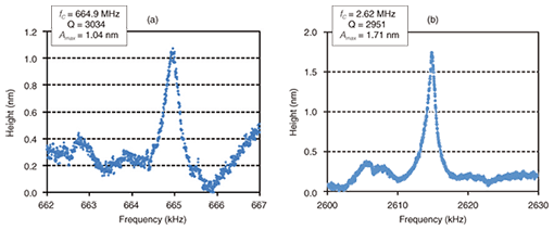
4. Experimental results and discussion4.1 Vibration analysesVibration analyses were performed near the center of the GaAs membrane resonator. The vibration characteristics of the membrane resonators are shown in Fig. 5. The frequency of the actuation voltage Vact was swept as a function of time, while the vibration amplitude in the z-direction was monitored as height information by the SPM system. Figure 4(a) shows the fundamental mode of the 65-µm-diameter membrane resonator, whose measured resonant frequency was 664.9 kHz and Q factor was 3034. The fundamental mode of the 26-µm-diameter membrane is presented in Fig. 5(b): the resonant frequency was 2.62 MHz and the Q factor was 2951. The actuation voltage in Fig. 5(a) was 60 mV while that in Fig. 5(b) was 300 mV. Thus, we could successfully detect and actuate vibration of the resonator using the SPM probe.
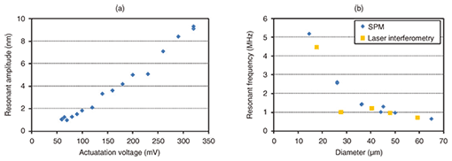
Figure 6(a) shows the relationship between the resonant amplitude and actuation voltage of the 65-µm-diameter resonator shown in Fig. 4(a). The resonant amplitude increased linearly with increasing actuation voltage. Figure 6(b) shows plots of resonant frequencies versus membrane resonator diameter measured by the SPM method (diamonds) and laser interferometry (squares). The SPM-measured frequencies were almost the same as the interferometry-measured ones. The GaAs membrane resonators vibrated at the same frequency as that of the actuation voltage. These results for amplitude and frequency suggest that the Coulomb force between the metal probe and the semiconductor membrane plays an important role in exciting the vibration.
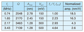
If a membrane is metal, then the exciting force generated by applying voltage Vact is the electrostatic force Fel , where Fel and Vact are linked by the relation Fel ∝ Vact2 [11]. If the mechanical quality factor Q is constant, the resonant amplitude Amax is proportional to Fel. Consequently, in the electrostatic force model for the metal membrane, Amax should be proportional to Vact2. Moreover, the frequency of Fel should be twice the driving frequency of Vact. However, for a semiconductor membrane, such as non-doped GaAs, an electrostatic force cannot be generated because carriers in the semiconductor cannot respond to a high-frequency electric field. Fixed charges in the GaAs layer, which originate from residual impurities or the surface state in molecular beam epitaxy growth [12], [13], play a significant role. The Coulomb force Fc is generated between an oscillating voltage Vact applied from the probe and fixed charges in the semiconductor membrane. In the Coulomb force model, the resonant amplitude Amax is proportional to Fc. Therefore, Amax should have a linear relationship with Vact. Furthermore, the force frequency of fc should be equal to the driving frequency of Vact. The experimental results shown in Fig. 5 agree well with the Coulomb force model. 4.2 Higher-order vibrationThe resonant frequency of a circular membrane resonator is given by the following formula [14]. 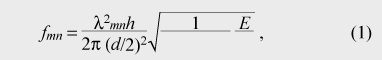 where λmn is the vibration constant determined by the vibrational mode, h is the membrane thickness, d is the membrane diameter, ν is Poisson’s ratio, E is Young’s modulus, and ρ is the material density. The ratios of higher-order modes to the fundamental mode (fmn/f00) are 2.08, 3.42, and 4.64 in decreasing order. The resonant properties of the measured fundamental and higher-order modes of the GaAs membrane resonator with dimensions d=65 µm and h=200 nm are listed in Table 1. The resonant frequency range of this membrane was from 0.74 to 3.43 MHz. The ratios of the higher-order modes to the fundamental mode were 2.23, 2.93, and 4.64. These deviations of the measured ratios from the described theoretical values are attributed to the effects of holes or strain [15].
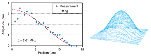
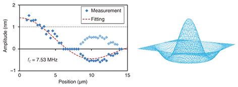
The normalized amplitude, which is defined by Amax/Vact, decreased with increasing frequency of the higher-order modes. Higher-mode vibrations are difficult to excite because of their larger effective spring constant. At this point, the maximum applied voltage Vact, which is 10 V, is a limiting factor for high-order mode excitation and detection. The maximum measurable frequency of the fundamental mode is also limited to about 10 MHz. More efficient exciting conditions and lower-noise detection techniques will improve the measurable limit of vibration. Note that there is no limitation on the actuation frequency in this method, unlike in conventional optical methods such as laser interferometry. A smaller, thinner membrane, such as a graphene nanomembrane [16], will be suitable for this SPM-based method. 4.3 Mapping of waveform distributionSince an SPM has nanometer-order spatial resolution, we expect our method to enable the mapping of the waveform distribution of nanoresonators [7]. The displacement distribution will improve our understanding of the mechanical properties of nanoresonators. Figures 7 and 8 show amplitude distributions of the fundamental mode and a higher-mode of the 26-µm-diameter membrane shown in Fig. 4(b). Dotted lines are calculated waveforms for a circular membrane. The actuation voltage Vact was kept constant for each measured point. Good agreement between the measured and calculated amplitude distributions is important for future applications, such as Young’s modulus determination and accurate calibration of mass, force, and charge sensing.
For a tapping force of 5 nN and tip radius of 30 nm, the probe-sample contact radius was estimated to be about 1 nm [17], which is much smaller than the spot size of optical systems. This means that the present method has the potential to determine the mechanical properties of much smaller areas than conventional methods. A more detailed investigation will help us understand the effect of very small defects or strain in nanoresonators induced by the fabrication process. 5. ConclusionsWe detected nanometer-order amplitudes at megahertz-order frequencies using a vibration analysis method where vibration actuation and detection are performed simultaneously using the probe of an SPM. An accurate vibration analysis can be performed without any probe interaction effect. We have shown that the waveform distribution of the fundamental and higher-order modes can offer a new perspective on the effects of nanometer-order mechanical structures, such as defects and strain. Since the experimental setup of our technique is very simple, this SPM-based technique should be a powerful tool for vibration analyses of nanoresonators. AcknowledgmentWe are grateful to Dr. Reo Kometani of the University of Tokyo for his FIB fabrication and helpful discussion. This work was partly supported by Grants-in-Aid for Scientific Research or KAKENHI from the Japan Society for the Promotion of Science (19206016, 19310085, 20246064, and 22310086). References
|
||||||||||||||||||||||||||||||||||||||||||||||||