|
|||||||||||||||||||||||||||||
|
|
|||||||||||||||||||||||||||||
       |
Feature Articles: Ultrahigh-speed Ultrahigh-capacity Optical Transport Network Vol. 9, No. 8, pp. 21–27, Aug. 2011. https://doi.org/10.53829/ntr201108fa3 Photonic Network Node Technology for Transparent Path AccommodationAbstractIn this article, we introduce research and development trends related to optical-electrical hybrid nodes. Meeting the demands for higher channel capacities, by for example wavelength division multiplexing at 100 Gbit/s per wavelength, will require not only optical switching of optical paths at photonic nodes, but also sub-lambda (electrical path) technology for multiplexing/demultiplexing and switching 1–10 Gbit/s medium-sized electrical paths. 
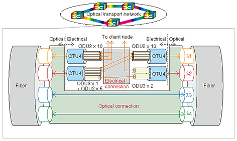
1. IntroductionThe photonic network can provide high-quality delivery of user traffic via optical paths over long transmission distances. This is achieved by assigning wavelength-based identifiers to the optical paths. In this article, we describe three main trends concerning new requirements related to photonic nodes. 1.1 High-capacity optical pathsThe use of advanced digital signal processing enables a spectral efficiency of 2 bit/s/Hz to be achieved, enabling long-distance transmission with a capacity of 10 Tbit/s (100 Gbit/s × 100 wavelengths) [1]. On the other hand, the input-output signals of client nodes, which contain user traffic multiplexed at edge routers, are expected to still be at the 10-Gbit/s level (10-Gbit/s Ethernet (10GbE)) in the mainstream in the near future. Therefore, the photonic nodes for these signals will need functions not only for optical multiplexing/switching of large optical paths, but also for electrical multiplexing/switching of medium-sized electrical paths, where the medium-sized electrical paths are aggregated into a large optical path. In other words, we need a multilayer processing function that can handle both optical and electrical paths in one node. The conceptual scheme for the optical-electrical hybrid node, with reference to the international standard for the Optical Transport Network (OTN), is shown in Fig. 1. The optical channels (wavelengths) conform to a digital frame format called an optical-channel transport unit (OTU) containing optical-channel data units (ODUs) [1]. An important point is that a client signal is wrapped into ODUs transparently, without any overwriting of the client overhead. NTT was the first in the world to achieve optical and electrical transparent-multiplexing technology for the OTN and has been leading the world in international standardization.
In this simple example in Fig. 1, four wavelengths are multiplexed in a single fiber. The first wavelength (λ1) contains an OTU4, which accommodates 10 × 10G electrical paths (ODU2), where the ODU2s are demultiplexed from a single ODU4 after optical-to-electrical (O/E) conversion and connected to the electrical (ODU) switching fabric (G: denotes Gbit/s). In the ODU switching fabric, each ODU’s route is provisioned, either to drop into a tributary port*1 or to continue into the express port. The express ODU2s are then multiplexed into a single OTU4 again, and converted (by optical-to-electrical (E/O) conversion) into a single optical path of wavelength λ1. The second wavelength (λ2) contains 2 × 40G electrical paths (ODU3), and they are connected to the ODU switching fabric. The third and fourth wavelengths (λ3 and λ4) are connected to the optical switch without O/E/O conversion.
1.2 IP traffic off-loading by cut-through in photonic nodeThe photonic network deployed to date has the simple role of connecting Internet protocol (IP) core routers. In all core networks, each IP core router has a multihop configuration, and the photonic networks are segmented sub-networks that are finely divided into small domains in a core network. With the target of low cost of overall networks, if we analyze the contents of core router processing, we begin to understand that it is often the case, in core routers, that traffic at the input port is simply forwarded to a fixed output port by means of a Layer-3 function. By providing cut-through technology at relatively low layers (optical and electrical paths), these simple functions can efficiently decrease the cost and power consumption. 1.3 Multidegree photonic nodesUnlike ordinary telephone traffic, IP (Internet) traffic has a tendency to be concentrated in large cities such as Tokyo and Osaka (and beyond Tokyo, there are many instances of connection to international circuits). To a certain extent, establishing multiple sets of equipment in different locations around a large city is known to be an effective decentralization method. The problems facing this configuration are that, since traffic increases are becoming unpredictable as a result of recent Internet characteristics, it is difficult to give a precise design target for the path capacities to be handled at each node. Therefore, we need flexibility in handling paths, e.g., some spare bandwidth and a mechanism for sharing it among nodes at different locations. If the traffic increases and exceeds the spare bandwidth prepared at a particular node, it will be even more necessary to disperse the traffic to other nodes at different locations while minimizing the difference in latency. The existing reconfigurable optical add/drop multiplexers (ROADMs) that support a node degree of 2 may be insufficient. A photonic node that supports multidegree switching would let us deal flexibly with this type of unpredictable demand. Another need is the ability to deal with disaster recovery. If we consider the effect of calamities such as earthquakes on the social infrastructure, e.g., on Internet commerce, it is not enough to have only two routes, i.e., the currently used working route and one backup protection route. We need to reserve a third route. For this purpose, photonic nodes that support multidegree switching are important. 2. Optical layer switching technologyHere, we introduce a function that meets the need for optical layer switching that arises from the new demand mentioned above and technology that enables the function. In photonic nodes, a multilayer configuration, i.e., with both optical and electrical switches, means that hybrid operation is needed, and an important issue is designing the electrical switch capacity because it represents a large proportion of the cost and power. One important point is what percent of the total transmission capacity of the fiber to allocate to electrical switching. In a practical design, we should carefully consider the traffic pattern etc., but from a functional perspective at least an arbitrary wavelength of an add/drop optical path should be connected to an arbitrary port of an electrical switch. As mentioned earlier, not only are existing ROADMs limited to a node degree of 2, but also the relationship between the add/drop wavelengths and tributary ports is fixed. In other words, when provisioning an optical path, after determining the established wavelength, operators must physically go to the add/drop equipment and insert the interface board in the port assigned to that wavelength. At an optical electrical hybrid node, the interface between the add/drop optical path and electrical switch port is inside the equipment, and operators generally do not touch the intra-connections once initial construction has been completed because of the vendor-dependent node configuration (the risk of misconnection might increase in different ways as a result of manual setting depending on the vendors).
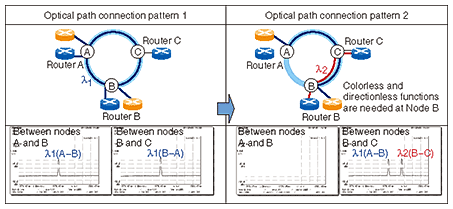
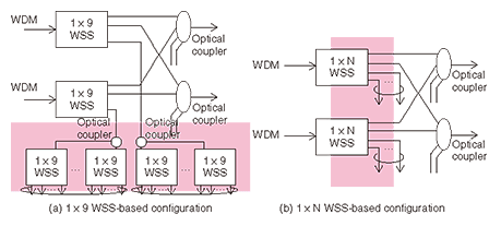
The technology that enables connections from a remote site, among arbitrary wavelength add/drop optical paths and arbitrary tributary ports, is called colorless. A similar function that deals with an add/drop optical path from an arbitrary express direction is referred to as directionless. Furthermore, in order to achieve directionlessness in the optical layer, there is a special methodology that avoids interference in a device among optical paths of the same wavelength called contentionless. An overview of the colorless-directionless demonstration conducted at NTT is shown in Fig. 2 [2]. A bidirectional ring network was used in the demonstration. As the initial operating state, optical path λ1 was established between node A and node B along the shorter route, and a different optical path was established between nodes B and A along the longer route with the same wavelength as λ1 (pattern 1). Although both optical paths had the same wavelength, the first path was protected from interference by the second path. In the optical spectra at the bottom of the figure, the wavelength in each route is active. In the next phase of the demonstration (pattern 2), the optical path between nodes A and B in the shorter route became unnecessary: instead, it was assumed that a demand for connection from node B to node C arose. Since λ1 was already active in this B-to-C route, wavelength λ1 could not be used. A different wavelength had to be used (λ2). Through the colorless directionless optical switch used in this demonstration, we showed remote resetting of the wavelength to meet new demands without physical replacement of the interface board. In pattern 2, two wavelengths were active in one route. A more detailed example of a colorless node configuration is shown in Fig. 3. The wavelength selective switch (WSS) shown in the figure is a device that enables switching of an arbitrary combination of WDM input signals to any combination of WDM output signals. To date, the 1 × 9 type WSS module has typically been used. To achieve the colorless function (Fig. 3(a)) by using the combination 1 × 9 WSS modules, the upper WSS establishes an optical path connection from an express-port to another express-port or from an express-port to an add/drop port connection. The lower WSS is for a path connection from an add/drop port to a tributary port. In this configuration, the number of modules is increased and each module incurs optical loss. Therefore, an optical amplifier is needed to compensate for the loss. A multiport (1 × N) WSS is currently under development; its configuration is shown in Fig. 3(b). This simple configuration will have fewer modules and a lower cost. We are verifying the principle of a 1 × 43 WSS and conducting verification experiments on the colorless function.
3. Electrical layer switching technologyAttention to electrical switch technology in the OTN is currently focused on Layer-1 technology and also packet-oriented Layer-2 (sometimes referred to as Layer-1.5) technologies using, for example, multiprotocol label switching transport profile (MPLS-TP)*2 or provider backbone bridge traffic engineering (PBB-TE)*3. There is high affinity between OTN and the synchronous digital hierarchy (SDH)*4 in terms of Layer 1 and also between MPLS-TP (PBB-TE) and asynchronous transfer mode (ATM)*5 in terms of Layer 2 (or 1.5), where carriers have the benefit of familiar network operation in practical use. Here, we introduce electrical-layer (Layer-1) switching and the hitless protection switching technique, which is important to NTT’s networks.
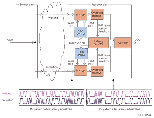
The OTN frame is constructed with reference to the digital-frame format stipulated in ITU-T Recommendation G.709 (ITU-T: International Telecommunication Union, Telecommunication Standardization Sector). This digital frame is a widely used format and is already becoming established in worldwide de jure and de facto standards. NTT previously developed an OTN framer LSI (large-scale integrated circuit) that could handle 40 Gbit/s [3], and the LSI took a large share of the world market after its commercialization. For the OTN, a multiplexing hierarchy is defined, and the ODU, which is a path in an OTN, is multiplexed/demultiplexed in fixed byte units. Therefore, an ODU switch should be of the circuit-switching type such as SDH. On the other hand, unlike SDH, the clock domain is sometimes not synchronized in frequency, and a device configuration that uses a frame buffer memory (first-in, first-out (FIFO)) is frequently used. This was triggered by the recent proliferation of personal computers leading to the availability of low-cost compact memory. Accordingly, there are two proposed ways to configure the ODU switch: the first is a circuit switching fabric whose capacity is extended from the ordinary one, and the second uses a packet switching fabric to achieve the ODU circuit switching function. In the latter case, the purpose of using the packet switching fabric is to take advantage of the lower cost of ICs achieved by the large production volumes shared with local area network (LAN) application. No conclusion had been reached yet on which way is better. Fault restoration and rerouting can be handled in the OTN layer, and at NTT Innovation Laboratories, we are investigating hitless protection switching technology, which is important to NTT’s networks. An overview of the hitless protection switching scheme is shown in Fig. 4. Basically, the same types of technologies as used in SDH can be applied to it. Namely, a multiframe is constructed by gathering digital ODU frames. This scheme achieves switching without any bit loss by detecting the difference in latency between the working and protection routes from the headers of these multiframes and by absorbing the latency difference in the buffer memory. In the ordinary hitless protection scheme, the protection route is predetermined, and switching should be based on 1+1 protection. On the other hand, we are extending the hitless protection scheme from the ordinary version to one in which an arbitrary non-predetermined protection route is possible (and the latency is not known in advance), which would be suitable for multidegree nodes because it provides multiple candidates for the protection route. By shifting the working clock frequency in a very slight range (sub-parts-per-million (ppm) order) while maintaining compliance to the standard ±20 ppm for the frequency shift, this scheme changes the phase (latency) of the current data. The configuration of a demonstration of this technology is shown in Fig. 4 together with the relationship between the working path data phase and the protection path data phase before and after latency adjustment. Here, the blue blocks represent the new scheme and the brown blocks represent the existing scheme to which the OTN frame is applied. After latency adjustment, the data phases are synchronized, and in the experiment, we verified that there was no bit loss during the switching.
4. SummaryAs a new direction in photonic nodes, this article described new technological trends in optical-electrical hybrid nodes that are the focus of research and development trends in our group in NTT Network Innovation Laboratories. Besides the technologies described here, we are also conducting research on efficient resource (bandwidth) usage based on control over multiple layers and on a transmission node that enables bitrate and bandwidth flexibility. Our activities are continuing to put into practice long-term research and development to achieve an economical flexible network configuration in the future. References
|
||||||||||||||||||||||||||||