|
|||||||||||||||||||||||||||||||||||||||||||||||||||||||||
|
|
|||||||||||||||||||||||||||||||||||||||||||||||||||||||||
       |
Regular Articles Vol. 10, No. 2, pp. 45–51, Feb. 2012. https://doi.org/10.53829/ntr201202ra1 Acoustically Controlled Spin Precession Revealed by Two-dimensional Imaging of Spin Transport in GaAsAbstractMagneto-optic Kerr microscopy was used to investigate the spin precession of electrons traveling in semiconductor quantum wells by using surface acoustic waves (SAWs). Two-dimensional images of the SAW-induced spin flow reveal anisotropic spin precession behavior caused by the coexistence of different types of spin-orbit interactions. The dependence of spin-orbit effective magnetic fields on SAW intensity indicates the existence of acoustically controllable spin-orbit interactions resulting from SAW-induced strain and SAW-induced Rashba contributions. These phenomena will provide the versatility needed for spin manipulation in future spintronic applications such as spin transistors and quantum computers. 
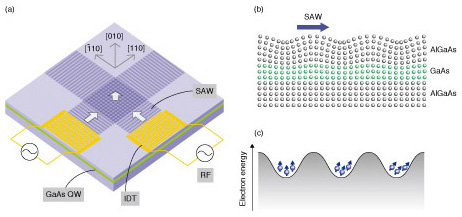
1. IntroductionIn conventional semiconductor electronics, electron spins have been ignored because they are randomly oriented and cancel out completely. The research field called semiconductor spintronics aims to extract spin properties in order to use them for both classical and quantum information technologies, which will achieve higher processing speeds, lower electrical power consumption, and higher integration densities than conventional charge-based devices [1]. Understanding the spin dynamics of electrons moving in semiconductors is one of the keys to developing spintronic technologies because it will enable electrical spin manipulation without external magnetic fields in ways that have been proposed for spin field-effect transistors [2], spin filters [3], and quantum computers [4]. In a system lacking inversion symmetry, moving electrons feel effective magnetic fields even in the absence of real magnetic fields. This is caused by spin-orbit interactions (SOIs) arising from relativistic effects. In general, magnetic fields induce spin precession, which is the rotation of the spin angular momentum around the magnetic field. Because of this, moving spins precess with a frequency proportional to the strength of the SOIs. So far, spin transport experiments using a DC-electric field [5] have succeeded in observing the spin precessions induced by SOIs in the absence of a real magnetic field [6]. Surface acoustic waves (SAWs) applied to semiconductor quantum wells (QWs), which confine electrons in thin layers sandwiched between barrier layers made of other materials, provide another way to transport electron spins [7]–[9]. This method has the advantage of effectively suppressing the dominant spin relaxation process caused by the electron-hole exchange interaction in undoped semiconductors [10] owing to the spatial separation of electrons and holes in the type-II-like lateral potential modulation created by the SAWs [7]. As a result, it has become possible to transport electrons by using SAWs over distances of nearly 100 µm while maintaining their spin coherence during precession around the effective magnetic fields caused by SOIs [8]. Here, we used magneto-optic Kerr rotation (KR) microscopy to explore the two-dimensional (2D) dynamics of traveling spins under SAWs over a wide range of acoustic amplitudes. The present experiment revealed the existence of spatially anisotropic SOIs as well as their dependence on SAW strength. A theoretical analysis of the experimental results elucidated the mechanisms of the acoustically controllable spin dynamics. The phenomena will provide a new approach for the spin-manipulation as well as spin transport without the application of any magnetic fields or DC electric fields. 2. ExperimentA schematic view of the sample is shown in Fig. 1(a). It was a 20-nm-thick undoped GaAs single QW with short-period GaAs/AlAs (average Al content: 30%) barriers grown by molecular-beam epitaxy on a (001) semi-insulating GaAs substrate. The QW was located 485 nm below the surface. A 50-nm-thick Al film deposited on top of the sample was processed by electron-beam lithography into interdigital transducers (IDTs), which were designed for operation at a SAW wavelength of 2.55 µm and frequency of 1.154 GHz. Rayleigh SAWs propagate along either [110] or [¯110], depending on the direction of the applied radio frequency (RF) signal, with a SAW velocity |vSAW| = 2.9 km/s. The single SAW beams produce moving wires, which are formed by the one-dimensional (1D) lateral confinement of the SAW-induced piezoelectric potential (Figs. 1(b) and (c)). Interference between two orthogonal SAW beams forms moving dots traveling along [010] with a velocity of
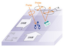
The spin dynamics during transport was measured by temporally and spatially resolved KR microscopy using a mode-locked Ti:sapphire laser (1.5 ps, 82 MHz, 1.527 eV), as illustrated in Fig. 2. Circularly polarized pump pulses (average power: 1.1 µW) were focused at a fixed position on the sample. Linearly polarized probe pulses (0.9 µW) with a time delay relative to the pump pulses were scanned over the surface and the KR angle θK of their reflected light was measured by a balanced detection technique. The pump light’s polarization was modulated between left- and right-circular polarizations at 50.1 kHz, and the probe light was chopped with an acousto-optic modulator at 52.0 kHz. The difference frequency (1.9 kHz) was used as a reference for lock-in detection. The full width at half maximum (FWHM) spot size of the normally incident probe beam was approximately 3 µm, whereas the waist size of the obliquely incident pump beam was 6 µm and its spot on the sample was slightly elongated in the [100] direction. The position of the probe light spot was scanned in the QW plane for spatially resolved KR measurements. For the 2D mapping of steady-state spin distributions, we chose to use a two-color pump-probe method using a pair of continuous-wave Ti:sapphire lasers. All the measurements were carried out at a low temperature (30 K), where long-distance spin transport is expected [7], [8] in the absence of applied magnetic fields.
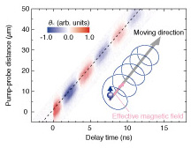
3. Results and discussionThe spatiotemporal evolution of photoinjected spins trapped in moving dots traveling in the [010] direction is shown in Fig. 3. The slope of the KR signal indicates that the spin-polarized electrons moved with the expected velocity of
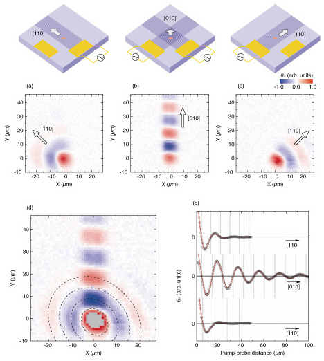
Spatial maps of steady-state spin densities for moving wires are shown in Figs. 4(a) and (c) and that for moving dots is shown in Fig. 4(b). In the two-color measurement, the pump energy was fixed at 1.527 eV, whereas the probe energy was tuned to 1.525, 1.526, and 1.528 eV for [¯110], [010], and [110], respectively, because the bandgap energies at the electron-trapping positions were modulated by SAW fields [11]. The pump (probe) power was 20 (0.9) µW. In contrast to the well-confined carrier transport achieved by moving dots (Fig. 4(b)), carriers in moving wires diffused rapidly along the wire axis (Figs. 4(a) and (c)). Although the KR signal for the wires was reduced by the carrier diffusion, we could access the momentum direction dependences of spin precessions (Fig. 4(d)), where the sum of the mapping data (Figs. 4(a)–(c)) shows that the isophase lines have clear elliptical shapes. In Fig. 4(e), the KR angles θK (open circles) along particular axes ([¯110], [010], and [110]) are fitted with a function θK(d)=θ0 cos(2πkd) exp(–d/Ls), where d is the pump-probe distance and Ls and k are fitting parameters representing the spin decay length and spatial precession frequency, respectively. We obtained k[110] = 0.0589 ± 0.0008, k[010] = 0.05369 ± 0.00009, and k[¯110] = 0.0460 ± 0.0006 µm–1 for the traveling directions [110], [010], and [-110], respectively. Since k is proportional to the spin-orbit effective magnetic field, these results demonstrate that the SOIs are spatially anisotropic in the present system.
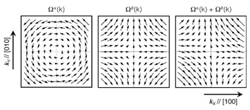
The SOI dependence on the traveling direction is caused by the coexistence of different types of SOIs [6], [12]–[14]. For electrons confined in (001) QWs, the momentum-dependent effective magnetic field Ωso(k)is primarily determined by k-linear terms, which are classified into two types [15]:  where we used a coordinate system with base vectors Xˆ // [100], Ŷ // [010], and Zˆ // [001]. The orientation dependences of Ωα(k) and Ωβ(k) in k space are shown in Fig. 5. Since these vectors have different dependences on the direction of k, their coexistence leads to twofold symmetry of |Ωtotal(k)|=|Ωα(k)+ Ωβ(k)|, as illustrated in Fig. 5. In general, Ωα(k) and Ωβ(k) are mainly induced by the structural inversion asymmetry caused by a static electric field (Rashba SOI [16]) and the intrinsic bulk inversion asymmetry (Dresselhaus SOI [17]), respectively. In addition to these static contributions, the present system should have a dynamic Rashba SOI induced by the vertical component of the SAW piezoelectric field as well as strain-induced SOIs [18]–[20].
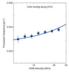
As expected, the precession frequency varied with the SAW intensity, which is defined as the acoustic power flux per unit length along a cross-section of the SAW beam. The symbols in Fig. 6 represent the experimentally obtained precession frequency as a function of the SAW intensity for moving dots. We estimated the SAW intensities from the bandgap shift observed in photoluminescence spectra [21]. As the SAW intensity increased, the precession frequency increased monotonically, suggesting that the SOI is acoustically controllable. The experimental data were well reproduced by simulating the precession frequency (solid lines in Fig. 6) [22], where each SOI contribution to the spin precessions was estimated from the calculation of the Rayleigh SAW fields including the piezoelectric coupling [23]. This analysis revealed the contributions of SAW-dependent Rashba and strain SOIs to the total SOI, indicating that the spin rotation angle can be tuned by adjusting the SAW intensity.
4. ConclusionWe studied the SOIs of electrons traveling in semiconductor QWs by using SAW fields. The temporally and/or spatially resolved KR technique enabled 2D imaging of the traveling spins, which revealed anisotropic spin precession behavior resulting from the coexistence of different types of SOIs. The dependence of the precession frequencies on SAW intensity, which was analyzed on the basis of a theoretical model, indicates that the strengths of the SOIs due to strain and Rashba contributions can be tuned by adjusting the SAW intensity. Our experimental results will be beneficial for further investigation of acoustically induced SOIs in semiconductors. They will also provide the versatility needed for spin manipulation via dynamically controlled SOIs in future spintronic applications such as spin transistors and quantum computers. AcknowledgmentsWe thank P. V. Santos of Paul-Drude-Institut für Festkörperelektronik, Berlin, Germany, and J. Nitta and M. Kohda of Department of Materials Science, Tohoku University, Sendai, Japan, for useful discussions. This work was partly supported by the Japan Society for the Promotion of Science (JSPS). References
|
||||||||||||||||||||||||||||||||||||||||||||||||||||||||