|
|||||||||||||||||||||||||||
|
|
|||||||||||||||||||||||||||
       |
Feature Articles: Circuit and Device Technologies for Extremely Low-power Consumption for Future Communications Systems Vol. 11, No. 2, pp. 35–40, Feb. 2013. https://doi.org/10.53829/ntr201302fa6 Vibrational Energy Harvesting with Microelectromechanical System TechnologyAbstractThis article introduces a system for converting ambient vibrational energy to electrical energy using a microelectromechanical system (MEMS). A novel slit-and-slider structure is proposed as a way to miniaturize small sensor terminals. The results obtained with this system are expected to pave the way to designing and fabricating small vibrational energy harvesters.
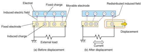
1. IntroductionDifferent sources of energy such as thermal energy, light energy, and vibrational energy exist in the ambient environment. Energy harvesting is a technology for capturing minute amounts of energy from one or more of these naturally existing energy sources in order to generate electrical energy from it and store it for later use. The harvesting of vibrational energy has been an area of particular interest and has been intensively studied because vibrational energy exists almost everywhere in our living environment [1]. Recent progress in various low-power-consumption technologies in the semiconductor field has made it possible to drive various circuits or devices with a tiny amount of energy. Consequently, the utilization of energy sources in the ambient environment has become a realistic possibility. Some groups in our laboratory have been researching sensor terminals and their low-power circuits for future ubiquitous sensor networks [2]. One of the fundamental technologies for these terminals that our group has been investigating is vibrational energy-harvesting technology using a microelectromechanical system (MEMS). This article describes the principle of converting energy from vibration, and reports on the fabrication and basic characteristics of a novel structure with a MEMS. 2. Fundamental process of energy harvesting with electrostatic conversion from vibrational energyThree types of energy conversion are possible when harvesting vibrational energy: electrostatic, piezoelectric, and electromagnetic [3]. Because we desire a power supply for various integrated circuits in a small sensor terminal, we chose electrostatic conversion because it is compatible with a planar process. An electrostatic energy harvester exploits the phenomenon of electrostatic induction by a dielectric. An electret is a suitable dielectric material because it can be charged to a high voltage and can hold the voltage semi-permanently on its surface. Electrets are used in many applications such as condenser microphones and air filters. The fundamental setup of the vibrational energy harvesting process using electrostatic induction with an electret [4], [5] is shown in Fig. 1. When negative charges are applied to the electret, positive charges are induced on a fixed electrode and a movable electrode (Fig. 1(a)). When the movable electrode plate is displaced by an external vibration in the direction of the arrow, some of the positive charges are moved from the fixed electrode to the movable one, and then current is generated through the external load (Fig. 1(b)). When positive charges are applied to the electret, negative charges are induced on the electrodes. This current is expressed as where, I, Q, and t are current, charge, and time. Assuming that the fundamental structure is an electrostatic capacitor model, we rewrite eq. (1) as where, V, C, ε, S, and d indicate voltage, capacitance, permittivity, the area of capacitance, and the gap of capacitance. The current increases as the gap of the structure becomes smaller, the area of the structure becomes larger, the constant of the electret material becomes higher, and the voltage of the electret becomes higher.
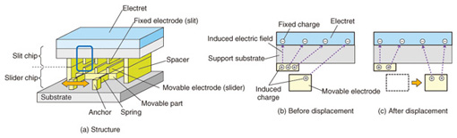
3. Novel structure3.1 DesignThe novel structure we devised [4], [5] is shown in Fig. 2. This structure, called a slit-and-slider structure, consists of an electret, a slit chip, which has fixed electrodes and physically supports the electret, and a slider chip, which has a movable electrode displaced by external vibration (Fig. 2(a)). The slit and slider chips are connected by a spacer to create a suitable gap between the fixed and movable electrodes. An illustration of part of the structure after the movable electrode moves is shown in Figs. 2(b) and (c). When negative charges are applied to the electret, positive charges are induced in the fixed and movable electrodes by an electric field that passes through the substrate (Fig. 2(b)). When the movable electrode is displaced to the right, some positive charges in the fixed electrode move to the movable electrode (Fig. 2(c)). AC (alternating current) between the fixed and movable electrodes is generated by the vibration of the movable part.
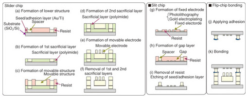
3.2 Fabrication processThe fabrication process for the device structure is based on thick-electroplating technology [6]. The fabrication process flow for the slit-and-slider structure is shown in Fig. 3. For the slider chip, first, the lower structures of the movable plate, for example, the lower interconnections, are formed on the substrate by gold (Au) electroplating (Fig. 3(a)). Next, the lower structures are planarized with photosensitive polyimide (Fig. 3(b)). The polyimide is a sacrificial layer that is removed later. Then, other parts of the movable plate and spacer are formed by repeating the electroplating and planarization steps (Figs. 3(c) to (e)). This stacking process simplifies the fabrication of the multilayered structure. Finally, the sacrificial layers are removed by dry ashing (Fig. 3(f)). The slit chip is fabricated using the same process. To bond the two chips, silver paste is applied to the walls of the slit chip, which is then flipped over and hot-pressed against the slider chip.
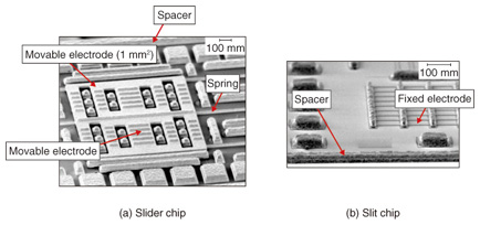
Images of fabricated slider and slit chips are shown in Fig. 4. The images were taken before the flip-chip bonding. Different elements for the slit-and-slider structure were fabricated on the substrate by stacking multiple layers. The movable plate is 1 mm2 in size and 20 µm in thickness, which makes it the smallest structure ever reported for an energy harvester with electrostatic induction.
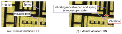
Close-up views of a movable plate on a chip without and with external vibration are shown in Figs. 5(a) and (b), respectively. When the movable plate moves vigorously because of the external vibration, a stroboscopic effect is observed for the movable plate and spring.
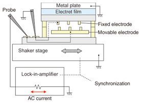
4. Energy harvesting experimentA schematic diagram of the experimental setup for current generation is shown in Fig. 6. The output from the movable electrode was connected to the input of a lock-in amplifier. The lock-in amplifier detects components with the same frequency as an input vibration reference signal. The surface of the electret was attached to the top of the slit chip, and the electret was fixed with a metal plate. The fixed and movable electrodes were interconnected separately outside the walls of the structure. The fixed electrodes and metal plate were connected directly to the ground. The frequency of external vibration was swept upwards, whereas acceleration was kept constant at 1 m/s2.
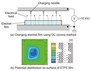
In this experiment, we used ethylene-tetrafluorinated ethylene copolymer (ETFE) film as an electret, because this material has long-term stability for holding charges [7], [8] and a good record of use in commercial products and applications [9]–[12]. The experimental setup for charging the electret film is shown in Fig. 7. The film was DC (direct current)-corona-discharged between a grounded electrode and high-voltage needle electrodes in this apparatus (Fig. 7(a)). The discharge was applied at –10-kV bias voltage at room temperature. The surface potential distribution of the charged film, which was set on the automatic two-axis stage, was measured with an electrostatic voltmeter. The measured potential distributions of the surface for each electret film are shown in Fig. 7(b). The surface potentials are about –450 V at minimum.
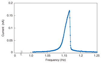
The current generation is shown in Fig. 8. The AC current is dependent on frequency. The current shows a peak at around 1.15 kHz. The maximum value is 0.17 nA at 1.17 kHz. This behavior coincides with the observation of the frequency characteristic of the movable part before flip-chip bonding, as shown in Fig. 5(b). Thus, the peak intrinsically comes from the resonant vibration. This result confirms that the vibrational device generates current with the electret.
5. ConclusionWe investigated a technology for vibrational energy harvesting using a novel slit-and-slider structure with electrostatic induction. We demonstrated through experiments that AC current was generated by external vibration and the electret. The maximum current was 0.17 nA at 1.17 kHz of external vibration with a magnitude of acceleration of 1 m/s2. These experiments show the potential of vibrational energy harvesting. This promising technology is expected to lead to the development of an energy harvester and sensor network terminals. References
|
||||||||||||||||||||||||||