|
|||||||||||||||
|
|
|||||||||||||||
       |
Feature Articles: Circuit and Device Technologies for Extremely Low-power Consumption for Future Communications Systems Vol. 11, No. 2, pp. 41–47, Feb. 2013. https://doi.org/10.53829/ntr201302fa7 Integrated Silicon-based Optical Interconnect for Fast, Compact, Energy-efficient Electronic Circuit SystemsAbstractThe performance of electronic circuit systems is now reaching saturation because of restrictions on the bandwidth, integration density, and power consumption of electronic interface devices. In this article, we present high-density chip-to-chip optical interconnects based on silicon photonics technology, which has the potential to solve these critical problems.
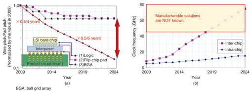
1. Optical interconnects in electronic circuit systemsThe information and communications industries are now facing an explosive increase in information processing capacity in order to support the distribution of heavy loaded rich content and the growing use of high-performance mobile terminals. The extensive construction of broadband network systems and huge datacenters has been carried out in order to cope with this information explosion. These large-scale information processing systems use an infinite number of electronic circuits, and it is therefore critical to improve their performance and reduce their power consumption. For example, the bandwidth of chip-to-chip interconnects between LSIs (large-scale integrated circuits) will double every two years and reach 1 Tbit/s in the mid 2010s and 10 Tbit/s in 2020 [1]. However, from the viewpoint of size and power consumption, such broadband interconnects cannot be achieved with conventional electrical wiring. The trend in the distance separating neighboring electrical wirings, which would determine the size of data interconnect systems [2], is shown in Fig. 1. For intra-chip interconnects, the separation can be reduced thanks to advances in microfabrication technology. For chip-to-chip interconnects, however, the separation must have some lower limit because the separation is determined by the geometrical structure of the pads and pins of LSIs, through which the LSIs are connected to printed circuit boards. Figure 1(b) shows the trend in signal frequency, which directly affects the power dissipation in electrical wiring. By the late 2010s, when the frequency is expected to reach 40 GHz, conventional electrical wiring will not be able to provide any practical solutions [2].
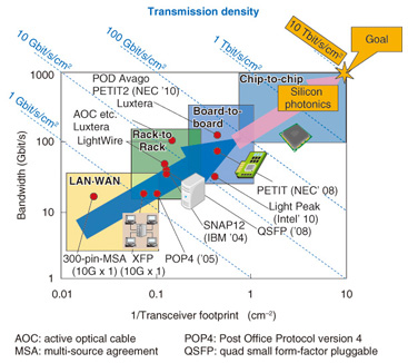
To solve these interconnect-related problems in electronic circuit systems, many organizations have developed optical interconnect technology. The relation between interconnect bandwidth and the footprint of interconnect modules [3] is shown in Fig. 2. Optical interconnect modules have conventionally been based on discrete photonic devices made of compound semiconductors and developed for applications in LANs (local area networks) and WANs (wide area networks) and for inter-rack and on-board interconnects. However, constructing a chip-to-chip interconnect system is very difficult with conventional photonic technology because it requires ultrahigh-density photonic device integration. Moreover, it is also very difficult with conventional photonic technology to converge photonics and electronics, which is one of the most important requirements in the optical interconnects. This is because materials, device sizes, design schemes, and fabrication processes in conventional photonic technology are quite different from those of electronics.
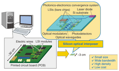
To solve these problems in conventional photonic technology and to construct a chip-to-chip optical interconnect system, we have developed a system using silicon photonics technology. This system can achieve high-density photonic device integration and has the potential for photonic-electronic convergence. 2. Concept of high-density optical interconnect systemA conceptual image of the high-density chip-to-chip optical interconnect system, or ultracompact optical interposer, is shown in Fig. 3 [3]. Laser diodes (LDs), optical modulators, and photodetectors (PDs) are integrated on a single silicon substrate and optically linked to each other by silicon optical waveguides. Bare LSI chips are mounted on the substrate and electrically connected to the optical modulators and PDs on the substrate by flip-chip bonding. Silicon photonics technology makes photonic devices ultracompact, and their integration density can therefore be significantly improved. The compact and high-density photonic device integration provides a compact optical interconnect system with large bandwidth and low power consumption. Moreover, CMOS (complementary metal-oxide semiconductor) electronics technology is used for most of the design and fabrication processes, which makes it easier to integrate discrete optical parts in the design and assembly processes. Thus, we can significantly reduce the costs of design and fabrication of integrated photonic devices.
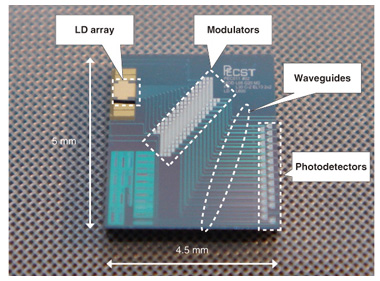
This technology will make it possible to achieve integrated silicon optical interconnect circuits with 10-Tbit/s/cm2 bandwidth in fiscal year 2013. 3. Fabrication of integrated silicon-based optical interconnect circuitsA photograph of the integrated silicon-based optical interconnect circuits we fabricated in 2010 [4] is shown in Fig. 4. The fabricated chip is 4.5 × 5 mm. A 13-channel (ch) LD array, silicon optical modulator array, and germanium (Ge) PD array are constructed on this chip, and these photonic devices are connected by silicon photonic wire waveguides. These devices are fabricated on a 4-inch silicon on insulator (SOI) wafer using a state-of-the-art fabrication process that is compatible with that for electronic circuits.
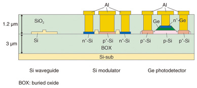
Cross-sectional structures of the photonic devices on the chip are shown in Fig. 5. The SOI layer, which forms the core of the silicon (Si) waveguide, is 200 nm thick. This SOI layer was used to fabricate 600-nm-wide silicon waveguide cores by electron-beam lithography and dry etching. Silicon optical modulators with a lateral p-i-n electronic structure were fabricated by implanting boron and phosphor ions. The silicon optical modulator is only 340 μm long, which is a few tenths the size of conventional ones made of lithium niobate crystals. Ge PDs were also fabricated by growing a Ge layer on the SOI layer and implanting boron ions into the Ge. The high-purity Ge layer was grown only in the region designed for the PDs by using the UHV-CVD (ultrahigh vacuum chemical vapor deposition) method.
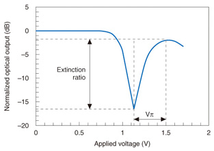
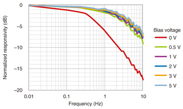
A silica overcladding layer was deposited on these optical modulators and Ge PDs by electron cyclotron resonance plasma-enhanced chemical vapor deposition (ECR-PECVD). The ECR-PECVD method allows silica layers to be deposited at temperatures below 200°C, which means we can form the silica overcladding layer without damaging the modulators and photodetectors underneath it. The silicon chip with the waveguides, modulators, and PDs was fabricated by NTT Advanced Technology Co. Waveguide facets and stages for LDs are formed on the fabricated chip by dry etching. Then, a 13-ch LD chip was mounted on the chip using a unique passive alignment method developed by PETRA (Photonics Electronics Technology Research Association) [5]. The wavelength of the LDs is in the 1.55-μm infrared band, which is widely used in telecommunications applications. 4. Performance of integrated silicon-based optical interconnect circuitsFirst, we present the performance of single devices fabricated on the chip. The measured optical attenuation performance of the Si modulator is shown in Fig. 6. The optical output power from the modulator was measured while applied voltage to the p-i-n structure of the modulator was swept. As shown in this figure, the VπL value, which represents the modulation efficiency of the modulator, is as small as 0.012 V • cm. A modulator with such a small VπL achieves low-voltage optical modulation. The extinction ratio of optical power is about 15 dB, which is large enough for optical data transmission [4]. Although the 3-dB frequency bandwidth of the modulator is a few hundred megahertz, the device can be used in operations of a few gigabits per second by applying a pre-emphasized input. The measured frequency characteristics of a PD are shown in Fig. 7. The 3-dB frequency bandwidth is 4.2 GHz, which is sufficient for receiving data at a few gigabits per second [4].
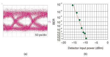
Next, let us look at the experimental results for the simultaneous operation of LDs, modulators, and PDs integrated on a chip. The 13-ch array of LDs was driven by a single DC power supply, and the continuous wave optical power from each LD was guided to an optical modulator. Digital signal data from a pulse pattern generator were pre-emphasized by an electrical differentiator and then applied to the modulator. The voltage of signal input to the modulator was 3.9 Vpp. The modulated optical signal was guided to the PDs and converted to an electrical signal. The experiment was performed under an uncontrolled temperature condition. An eye pattern of the output signal from the PD for a 5-Gbit/s NRZ (non-return-to-zero) data stream is shown in Fig. 8(a). The eye pattern is clearly open, which confirms the 5-Gbit/s data transmission capability in the on-chip integrated optical interconnection circuit [4]. No significant channel cross-talk was observed in the neighboring channels. The measured bit error rate (BER) in a 5-Gbit/s transmission operation is shown in Fig. 8(b). A BER of less than 10-12, or an error-free operation, was confirmed when the detector input power was -9.5 dBm.
In this silicon-based optical interconnection circuit, the sum of the footprints of an LD, modulator, and PD, including electrode pads, is estimated to be 0.144 mm2 per channel. Since 5-Gbit/s data transmission has been confirmed in one data channel, the transmission density of this optical interconnection system is estimated to be 3.5 Tbit/s cm2. This is a new world record for transmission density in an optical interconnection using light sources. 5. Toward 10-Tbit/s/cm2 interconnectsIn order to achieve our target transmission density of 10 Tbit/s/cm2, further improvement in the device performance and a reduction in the device size are necessary. For example, a 100% increase in operation speed and a 30% reduction in device size are required. To increase the operation speed, we have developed modulators with a side-wall grating structure. This structure improves optical confinement and reduces the width of the waveguide core, which directly contributes to increasing the modulation efficiency and speed. Moreover, we have developed PDs with MSM (metal-semiconductor-metal) electrode structures; these PDs also contribute to increasing the frequency bandwidth of the photodetector. To reduce the footprint of the LDs, we have developed a low-loss LD coupling structure and optical branches, which makes it possible to reduce the number of LDs while keeping the optical power per channel constant. Thanks to these improvements, we have already increased transmission density to 6.6 Tbit/s/cm2 [6]. For this result, the electrode pads, which occupy half of the device footprint, were still large because it was necessary to use measurement probes for testing. However, in practical interconnect systems, we do not need such large pads for the testing; therefore, we can significantly reduce the area of the electrode pads to achieve a 30% reduction in the total device footprint. With these improvements, we expect to achieve our final target, a 10-Tbit/s/cm2 transmission density, in the near future. AcknowledgmentThis research is supported by the Japan Society for the Promotion of Science (JSPS) through its Funding Program for World-Leading Innovative R&D on Science and Technology (FIRST Program). References
|
||||||||||||||