|
|||||||||||||||||||||||||
|
|
|||||||||||||||||||||||||
       |
Regular Articles Vol. 12, No. 11, pp. 97–103, Nov. 2014. https://doi.org/10.53829/ntr201411ra1 A 10G/1G Dual-rate Burst-mode Receiver for Next Generation Optical Access NetworksAbstractThis article describes a burst-mode receiver that is a key component of 10 Gigabit Ethernet passive optical network (10G-EPON) systems. In addition to coping with a burst signal, the receiver can operate at data rates of both 10.3125 and 1.25 Gbit/s to meet the need for coexistence of future 10G-EPON and existing Gigabit Ethernet PON (GE-PON) optical network units. The receiver sensitivities are –30.3 and –35.6 dBm at data rates of 10.3125 and 1.25 Gbit/s, respectively, when the receiver settling time is 400 ns. These results meet the 10G-EPON and GE-PON specifications with sufficient margins. Keywords: burst-mode receiver, 10G-EPON, transimpedance amplifier
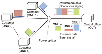
1. IntroductionThe number of subscribers of fiber-to-the-home (FTTH) services exceeds 25 million in Japan [1]. The Gigabit Ethernet passive optical network (GE-PON) [2] is now widely used for FTTH. However, since the data traffic of mobile, cloud computing, and ultra-high-definition (4K/8K) video services is expected to expand rapidly, the demand for bandwidth for optical access network services, including FTTH, is continuously increasing. Thus, an optical access network with higher bandwidth than that of GE-PON is needed. The 10 Gigabit Ethernet PON (10G-EPON) [3], which has ten times the bandwidth of GE-PON, is a promising candidate for the next generation optical access networks. The PON system is illustrated in Fig. 1. The main feature is that multiple customers share one optical fiber, which reduces the cost. An optical network unit (ONU) is installed on each customer’s premises, and multiple ONUs connect to an optical line terminal (OLT) in the central office. Downstream data are transmitted as a continuous signal. However, upstream data consist of asynchronous burst signals, and these bursts have different optical power levels and timings. Thus, it is essential that the OLT have a burst-mode receiver that can receive such optical burst signals and instantaneously amplify them to a fixed amplitude in an electrical signal.
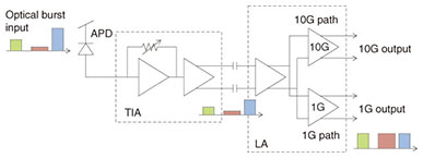
Such a burst-mode receiver requires high sensitivity, a wide dynamic range, and a short settling time in order to meet PON specifications. Another important issue is dual-rate operation. When upgrading the GE-PON to 10G-EPON, we have to be able to connect the 10G-EPON OLT to both 10G-EPON ONUs and existing GE-PON ONUs. Therefore, a burst-mode receiver for the 10G-EPON system, particularly in Japan, is strongly required in order to be able to receive 1.25-Gbit/s burst signals from GE-PON ONUs and 10.3125-Gbit/s burst signals from 10G-EPON ONUs as well. We describe in this article a 10G/1G dual-rate burst-mode receiver containing a burst-mode transimpedance amplifier (TIA) and limiting amplifier (LA). Careful and optimized design of automatic gain control (AGC) with a dummy circuit in the TIA and a 10G/1G dual-path configuration in the LA makes it possible to achieve sensitivities of –30.3 and –35.6 dBm at data rates of 10.3125 and 1.25 Gbit/s, respectively, and a settling time of 400 ns at both data rates. 2. Target performance of dual-rate burst-mode receiverSeveral burst-mode receivers have been studied in order to meet the requirements described above. To achieve wide dynamic range of more than 22 dB, which is specified in the 10G-EPON standard, the receiver gain must vary in accordance with the input optical power. That is, the gain should be large when the power is small and small when the power is large. Receivers are generally classified into two groups: those with continuous AGC and those with step AGC [4, 5]. The gain in continuous AGC varies continuously, whereas it varies discontinuously in step AGC. Generally, step AGC has two or three fixed gains. In a receiver with continuous AGC, a gain control signal tracks the average of the input signal power so that it can tolerate fluctuations in the power. Moreover, a reset signal that initializes the AGC circuit and is generally required in step AGC is not required in many cases. This leads to a simple receiver configuration. However, it requires a relatively longer settling time than that of step AGC. This is because it becomes difficult to tolerate long consecutive identical digits (CIDs) since the gain control signal tracks the average of the input power when the response time of continuous AGC is shortened in order to obtain a short settling time. A continuous AGC burst-mode receiver [6] achieved high sensitivities of –30.8 and –35.5 dBm in 10G and 1G operations, respectively, but needed a settling time of 800 ns in 10G operation. The receiver developed by Takahashi et al. [7] reduced the settling time to 400 ns, although the sensitivity for 1G operation stayed at around –30 dBm because the receiver architecture was not optimized for 1G operation. By contrast, in a receiver with step AGC, the settling time can be shortened to less than 200 ns [8, 9]. The receiver gain in step AGC is fixed in each step, so the receiver can obtain robustness to long CIDs even when the time constant of the AGC is short. However, step AGC requires a reset signal between each burst packet to initialize the gain. This reset signal should be a short pulse with a width of less than a few tens of nanoseconds, and the reset timing should be precise enough to correctly apply the reset at a gap of two bursts. This leads to a complex receiver configuration. A recently developed continuous AGC receiver achieved a settling time of 240 ns with high sensitivity by switching the time constant of the AGC [10]. The time constant in this receiver remains short before the reception of a burst signal in order to achieve a short settling time. After a burst signal arrives, the receiver detects the signal and then switches the time constant from short to long in order to handle long CIDs. However, the reset signal has to initialize the time constant of the AGC between each burst packet. The 10G/1G dual-rate burst-mode receiver presented in this article is a continuous AGC without a reset signal. We selected the time constant of the AGC carefully in order to achieve a settling time of 400 ns, which is half that specified in the 10G-EPON standard and the same as that specified in the GE-PON standard. Furthermore, the targets of the receiver sensitivity are at least –30 and –32 dBm at bit error ratios (BERs) of 10–3 and 10–12 at data rates of 10.3125 and 1.25 Gbit/s, respectively. These values are 2 dB better than that of the standards. To achieve high sensitivity, we optimized circuit parameters for both 10G and 1G operations. 3. Dual-rate burst-mode receiver architecture and circuit3.1 Receiver architectureA simplified schematic of our dual-rate burst-mode receiver, which consists of an avalanche photodiode (APD), TIA, and LA, is shown in Fig. 2. The APD converts an input optical burst signal into an electrical current signal. The TIA converts the current signal into a voltage signal and amplifies it. The LA amplifies various voltage amplitudes for each burst packet to a constant level.
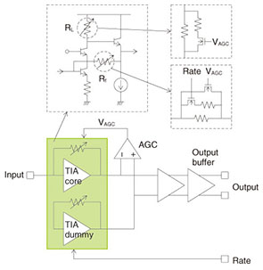
The TIA uses continuous AGC, which, as mentioned above, does not require a reset signal. The details are described in section 3.2. The LA has two signal paths: a 10G path for a rate of 10.3125-Gbit/s and a 1G path for a rate of 1.25-Gbit/s. The –3-dB bandwidth of the 1G path was designed to be 1 GHz to improve sensitivity at a data rate of 1.25 Gbit/s, while that of the 10G path was designed to be 8 GHz. The TIA and the LA are connected via alternating current (AC) coupling capacitors to cancel the signal offset. 3.2 Burst-mode TIAThe dual-rate burst-mode TIA circuit is shown in Fig. 3. Continuous AGC is used in the TIA to achieve a wide dynamic range and make a reset signal unnecessary. The first stage of the TIA has two identical circuit blocks: a TIA core and TIA dummy. The TIA core receives the input current signal. The TIA dummy generates a reference voltage equal to that of the output of the TIA core with no input current. The reference voltage from the TIA dummy is employed to cancel process, voltage, and temperature (PVT) variations, to generate a precise AGC voltage, and to cancel common mode noise. The AGC circuit averages the difference between the output voltages of the TIA core and dummy and then outputs an AGC signal, VAGC. When the input current is small, VAGC is low. This makes feedback resistance, Rf, and load resistance, RL, high, which results in a high TIA gain. This enables the TIA to receive a small input current. When the input current is large, VAGC becomes high. This makes Rf and RL low, which results in a low gain. In this way, the linear operation of the TIA is maintained, and the output signal is prevented from saturating and distorting even when the input current is large.
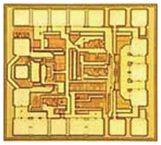
A rate signal is employed to optimize the sensitivity at each data rate. To obtain a high-sensitivity receiver, it is important to reduce the equivalent input noise current, ieq, of a TIA. Most of the ieq comes from Rf, and ieq becomes low as Rf becomes large. Thus, to obtain high sensitivity, large Rf is desired. However, large Rf limits the –3-dB bandwidth of a TIA because the bandwidth is inversely proportional to Rf. In other words, the optimum value of Rf is different at different data rates. Therefore, we employed a rate signal to change Rf according to the data rate. One of the most important parameters for burst-mode receivers is the time constant for AGC. A study showed that the time constant should be shorter than one-fifth of the receiver settling time and more than eight times the maximum number of CIDs [11]. Since the target for the settling time is 400 ns, the time constant should be less than 80 ns. The maximum number of CIDs in GE-PON and 10G-EPON is 5 and 66 bits because GE-PON and 10G-EPON use 8B/10B and 64B/66B coding, respectively. Consequently, the longest CID period is 4 ns in GE-PON and 6.4 ns in 10G-EPON, so the time constant should be larger than 50 ns. In other words, the –3-dB low-cutoff frequency of the frequency response of the receiver should be between 2 and 3 MHz. In our TIA, we designed the AGC loop to have a cutoff frequency of 2 MHz because we considered it important to have a tolerance to CIDs longer than 66 bits. 4. Experimental resultsA micrograph of the prototype TIA integrated circuit (IC) is shown in Fig. 4. The IC was fabricated by using a 0.25-µm SiGe BiCMOS (bipolar complementary metal-oxide semiconductor) process. The chip size is 1.1 × 0.99 mm2.
4.1 Frequency response of the TIAThe measured frequency responses of the TIA are shown in Fig. 5. The transimpedance gain, Zt, of the TIA was calculated from S (scattering) parameters obtained by on-wafer measurement. When we calculated Zt, we also took into consideration the parasitic capacitance of an APD and the inductance of the bonding wire between the APD and the TIA. The 10G and 1G modes indicated in Fig. 5 denote that the feedback resistance, Rf, is set small for 10.3125-Gbit/s operation and large for 1.25-Gbit/s operation, respectively, by using a rate input as described in section 3.2. As shown in Fig. 5, we obtained Zt of 66 and 76 dB, and a –3-dB bandwidth of 9 and 0.8 GHz in the 10G and 1G modes, respectively. These are sufficient gain values and bandwidths for 10G/1G dual-rate operation.
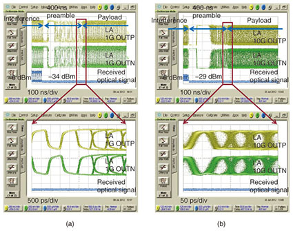
4.2 Performance of dual-rate burst-mode receiverThe TIA was mounted in a transistor outline (TO)-can package with an APD. A flexible printed circuit was soldered to the lead pins of the TO-can package as an electrical interface. The package was connected to the LA through the flexible printed circuit and AC-coupling capacitors, as shown in Fig. 2. Burst responses of the dual-rate burst-mode receiver from loud to soft bursts are shown in Fig. 6. The loud burst was used as an interference burst, and its optical power was –6 dBm, which is the same as the overload specified in the standards. This is the most severe condition for evaluating the settling time and sensitivity of burst-mode receivers. The soft burst was used as a measured burst consisting of a preamble and payload. The preamble pattern defined in the existing standards was used, and its period was 400 ns to confirm a receiver settling time of 400 ns. The payload patterns were 231-1 and 27-1 PRBS (pseudo-random binary sequence), and the input optical powers of the measured bursts (soft bursts) were –29 and –34 dBm at 10.3125 and 1.25 Gbit/s, respectively. Since these are lower powers than the receiver sensitivities specified in the standards, these values are sufficient for evaluating the settling time. In addition, the guard time between interference and measured bursts was set at less than 10 ns. As shown in Fig. 6, the receiver can respond in less than 200 and 300 ns for 1.25- and 10.3125-Gbit/s operations, respectively, which means the receiver has sufficient margin to achieve a settling time of 400 ns.
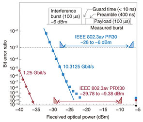
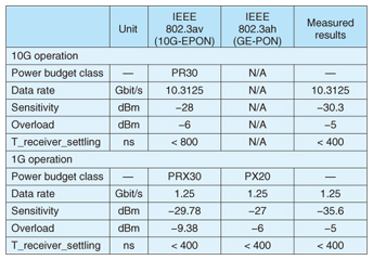
The measured BER is shown in Fig. 7. The data patterns used in the BER measurement are the same as described above. The measured sensitivities are –30.3 dBm at a BER of 10–3 and –35.6 dBm at a BER of 10–12 at 10.3125 and 1.25 Gbit/s, respectively. The sensitivity is more than 2 dB higher than that in the standards. The measured results and the standard specifications are summarized in Table 1. We confirmed that the receiver successfully meets the 10G-EPON/GE-PON standards.
5. ConclusionWe have developed a dual-rate burst-mode receiver that complies with 10G-EPON and GE-PON standards. The receiver sensitivities are –30.3 and –35.6 dBm at 10.3125 and 1.25 Gbit/s, respectively, with a settling time of 400 ns and without a reset signal by using a continuous AGC. These values are more than 2 dB higher than that in the standards. References
|
||||||||||||||||||||||||