|
|||||||||||||
|
|
|||||||||||||
       |
Feature Articles: Photonics-electronics Convergence Hardware Technology for Maximizing Network Performance Vol. 14, No. 1, pp. 19–24, Jan. 2016. https://doi.org/10.53829/ntr201601fa2 High-speed Electronic and Optical Device Technologies for Ultralarge-capacity Optical TransmissionAbstractTo increase the transmission capacity of optical fiber transmission systems, we have developed a multiplexer-digital-to-analogue converter and an optical time-division multiplexing modulator, which respectively generate high-speed signals in the electronic and optical domains. With these devices, we can significantly increase the capacity per wavelength channel. Keywords: DAC, modulator, QAM
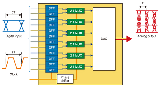
1. IntroductionThe demand for data transmission capacity is continuing to increase, and to meet this demand, optical transmission systems with per-channel rates exceeding 400 Gbit/s are desired. Several advanced technologies such as multicarrier transmission, high-order multilevel modulation, and high-symbol-rate transmission are expected to be key technologies for achieving a significant increase in capacity. In this article, we describe a multiplexer-digital-to-analog converter (MUX-DAC) and an optical time-division multiplexing (OTDM) modulator, which respectively double the symbol rates in the electronic and optical domains. 2. High-speed InP-HBT MUX-DAC2.1 Circuit configurationMultilevel modulation with a high baud rate is essential for achieving a channel capacity larger than 400 Gbit/s. The MUX-DAC combines the functions of a 2:1 multiplexer (MUX), which doubles the symbol rate, and a digital-to-analog converter (DAC), which converts the input binary (digital) signals to an output multilevel (analog) signal [1]. A functional-block diagram of the fabricated MUX-DAC with 6-bit resolution is shown in Fig. 1. The MUX-DAC operates as follows; first, the twelve input digital signals are synchronized with each other and reshaped by twelve D flip-flops (DFFs). Then, the outputs of the six pairs of DFFs are respectively multiplexed by six 2:1 MUXs, which generates six digital signals with a doubled symbol rate. Finally, the outputs of the MUXs are converted to an analog signal with a resolution of 6 bits. Since the frequency of the clock signal input to the DFFs and MUXs is half the symbol rate of the output analog signal, the MUX-DAC is suitable for high-symbol-rate applications. For the DAC section, we employed the R-2R ladder configuration to achieve high-speed operation with low power consumption.
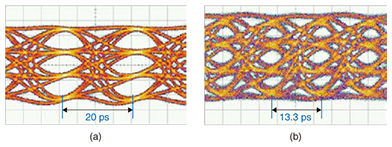
2.2 Fabrication and characteristicsWe have developed fabrication technologies for indium-phosphide (InP) heterojunction bipolar transistor (HBT) devices, which are promising for high-speed applications in photonic networks [2]. We used our InP HBT process with a linewidth of 0.5 μm to fabricate the MUX-DAC. With this process, we can achieve a very high cutoff frequency (a metric of the operation speed of a transistor) of 290 GHz. Power consumption of the MUX-DAC integrated circuit (IC) is 3.4 W, with roughly 2.9 W consumed in the DFFs and MUXs and only 0.5 W used in the DAC section. The differential output swing voltage is 1 V. The 3-dB bandwidth of the frequency response of the MUX-DAC module exceeds 40 GHz, which is currently the largest value in the world. Eye diagrams of the output four-level (2-bit) signals with symbol rates of 50 and 75 Gbaud are shown in Figs. 2(a) and 2(b), respectively. Clear eye openings were achieved at a symbol rate as high as 75 Gbaud.
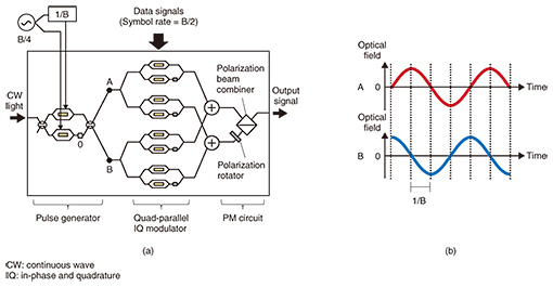
3. OTDM modulator with a silica-LN hybrid configuration3.1 Circuit configurationOTDM technologies have been extensively studied with the objective of breaking the limit of the speed of electronics and generating ultrahigh-speed optical signals. In an OTDM transmitter, each tributary signal (signal to be multiplexed) is shaped into a pulsed waveform to avoid interference between the tributaries. Our modulator, which is designed for an OTDM with two tributaries, combines the functions of a pulse generator and two data modulators [3]. Each data modulator is a dual-polarization optical vector modulator, which is the standard modulator in currently deployed 100-Gbit/s digital coherent systems. The OTDM modulator generates the output optical signal with a symbol rate that is double that of each input electronic signal. Unlike conventional OTDM setups, in which a pulsed light source and separate modulators are connected via fiber, the integrated OTDM modulator provides a much smaller footprint and higher stability of the relative optical phase between the tributaries. The OTDM modulator consists of a pulse generator, four optical vector modulators, and a polarization-multiplexing (PM) circuit, as shown in Fig. 3(a). Each of the two outputs of the pulse generator is bifurcated and sent to two of the four vector modulators. The outputs of each pair of vector modulators connected to different ports of the pulse generator are coupled, and the two coupled pairs are finally multiplexed in the PM circuit with orthogonal polarizations. The pulse generator consists of two Mach-Zehnder modulators (MZMs) connected in parallel with an output 2 × 2 coupler. To obtain a final output symbol rate of B, the two MZMs in the pulse generator are driven with sinusoidal clock signals with a frequency of B/4 and a relative delay of 1/B. Each vector modulator also consists of two parallel MZMs, which are driven with data signals with a symbol rate of B/2. As shown in Fig. 3(b), the intensity peak of the output from one port of the pulse generator always coincides with the extinction of the output from the other port and vice versa. Thus, we can transmit the two tributary signals without inter-symbol interference. Unlike the conventional OTDM with a pulsed light source, which is complicated and provides low spectral efficiency because of the broad spectral bandwidth of the pulse train, our OTDM modulator operates with a simple continuous-wave light source and offers higher spectral efficiency.
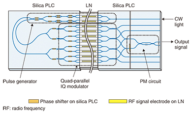
3.2 Fabrication method and characteristicsTo fabricate the OTDM modulator with the complex configuration shown in Fig. 3, we used a hybrid integration of silica planar lightwave circuits (PLCs) and a lithium niobate (LN) chip [4]. The hybrid integration enables us to obtain both high design flexibility for the silica PLCs and a broad electro-optic modulation bandwidth of the LN chip at the same time. The LN chip has ten push-pull pairs of straight phase modulators in an array, which corresponds to the ten MZMs: two for the pulse generator and eight for the four vector modulators (Fig. 4). All other passive components such as couplers, static phase shifters, and the PM circuit are fabricated in the PLCs. The pulse generator and the vector modulators are connected via U-turn waveguides to make the module compact. The modulator’s static insertion loss for both polarizations is 9.5 dB at a 1550-nm wavelength. All the MZMs have electro-optic 3-dB bandwidths of ~23 GHz. The half-wave voltage of each MZM is ~3.5 V.
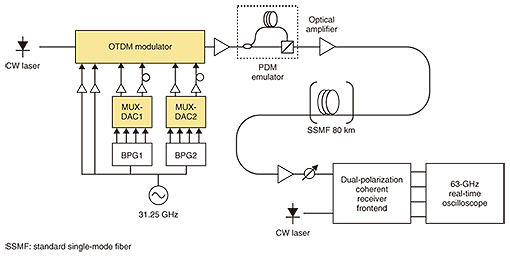
4. Large-capacity transmission experiment using the MUX-DAC and OTDM modulatorUsing the MUX-DACs and the OTDM modulator in combination, we can generate an ultralarge-capacity optical signal [5]. The experimental setup for a 125-Gbaud polarization-division-multiplexed (PDM) 16-level quadrature amplitude modulation (16QAM) signal generation using the two devices is shown in Fig. 5. The MUX-DACs converted 31.25-Gbaud binary signals (pseudo-random bit sequences) from bit-pattern generators (BPGs) into 62.5-Gbaud four-level electronic signals, which are used to drive the OTDM modulator to generate the 125-Gbaud 16QAM optical signal. Since only two MUX-DAC modules were available for the experiment, we drove only one polarization channel of the OTDM modulator and generated the PDM signal by using an external emulator. The optical signal was received by a coherent receiver with a 63-GHz real-time oscilloscope and demodulated offline to calculate the bit-error rate (BER).
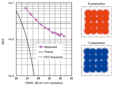
The measured back-to-back BER versus optical signal-to-noise ratio (OSNR) curve is shown in Fig. 6. We obtained BERs below 2.7 × 10⁻², which is the threshold of the forward error correction (FEC) code with 20% overhead, with an OSNR larger than 28.4 dB. We also tested transmission over 80-km standard single-mode fiber (SSMF) and obtained BERs below the threshold of 2.7 × 10⁻² with a launched power smaller than +14 dBm. Since the PDM-16QAM signal conveys 8 bits of information per symbol, the gross bit rate of the 125-Gbaud PDM-16QAM signal is 1 Tbit/s. Based on an assumed use of the FEC with 20% overhead, the net data rate is 800 Gbit/s. These values are records for single-carrier optical transmission using a single modulator (with an external PDM emulator).
5. SummaryWe developed a high-speed InP MUX-DAC and an integrated OTDM modulator with a silica-LN hybrid configuration, which double the respective symbol rates in electronic and optical domains. Using these devices, we successfully demonstrated the first 1-Tbit/s single-carrier optical transmission with a single modulator. These device technologies are promising for future ultralarge-capacity optical transmission systems. References
|
||||||||||||