|
|||||||||||||||||
|
|
|||||||||||||||||
       |
Feature Articles: Forefront Research on Bio-soft Materials Vol. 14, No. 8, pp. 33–37, Aug. 2016. https://doi.org/10.53829/ntr201608fa6 On-chip Graphene BiosensorAbstractThis article describes our recent research on an on-chip biosensor that uses the surface of graphene, an atomically thin carbon sheet modified with specific DNA (deoxyribonucleic acid) molecules, which binds selectively to a target molecule. Biologically important proteins such as cancer markers can be detected simply by adding a sample solution smaller than 1 microliter to the sensor chip. Quantitative detection of multiple proteins on a single graphene biosensor chip is demonstrated by using a microchannel configuration. Our findings have the potential to lead to a simple assay technique for disease markers. Keywords: graphene, biosensor, protein
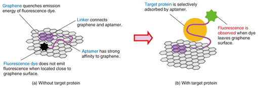
1. IntroductionGraphene is an atomically thin two-dimensional sheet consisting of a hexagonal honeycomb lattice of carbon atoms. It has been attracting great attention owing to its unique properties, which include extremely high mechanical strength, thermal conductivity, electronic mobility, and thermal and chemical stability [1]. Graphene was isolated in 2004 by Profs. Geim and Novoselov of the University of Manchester, who won the 2010 Nobel Prize in Physics for their pioneering work. The mass production of graphene was difficult at that time but has progressed greatly. It is now possible to obtain a monolayer of graphene several tens of centimeters square by using synthetic techniques typified by the chemical vapor deposition process. At the same time, graphene oxide (GO), the most widely known chemical derivative of graphene, is also attracting considerable interest. GO is an oxidized form of graphene, and it also has an atomically thin sheet-like structure, which contains nanometer-sized graphene-like domains. In GO, many of the bonds between the carbon atoms in graphene are broken and link with oxygen to form carbon-oxygen bonds. GO is prepared very differently from graphene and is rather easy to mass-produce. We can chemically synthesize GO by oxidizing graphite powder in strong acid. This yields a large quantity of GO in a glass container; however, it is difficult to obtain synthesized GO larger than a millimeter square. Therefore, GO is not suitable as a replacement for graphene in electronic materials that require high mobility, but is applicable to optical devices and sensing materials [2]. On the surface of graphene (or the graphene-like domains in GO), energy transfer occurs when molecules are located close to the surface. The energy transfer yield depends on the degree of molecular interaction between the adsorbed molecules and the graphene surface. For example, when a fluorescent molecule such as a dye is located very close to the graphene surface, the dye does not exhibit fluorescence. Here, graphene works as an excellent acceptor for fluorescence resonance energy transfer (FRET) over the entire visible wavelength region. By using the energy transfer reaction on a graphene surface, we can visualize biological/chemical reactions by converting those invisible molecular behaviors into the measurable physical quantities such as light and electricity. This makes graphene a promising material for a novel biosensor. We have proposed and developed a unique type of biosensor, which works on a graphene surface, by modifying it with a specific deoxyribonucleic acid (DNA) called an aptamer for the detection of biologically important proteins such as cancer markers (aptasensor, aptamer-based biosensor). We call a solid surface functionalized by biological molecules a biomolecular interface. First, we achieved biomolecular interfaces using GO and confirmed their usefulness for protein detection. We also fabricated on-chip sensors by combining the system with microfluidic techniques. Then we demonstrated protein detection by replacing GO with graphene to achieve an aptasensor with better performance than one with GO. 2. Mechanism of graphene aptasensorOur graphene aptasensor uses a graphene surface modified with an aptamer, which is a selected single-strand (ss) oligonucleotide that binds to a specific target. One end of the aptamer is labeled with a fluorescent dye, and the other end is connected to a pyrene linker molecule, which shows a strong affinity to the graphene (graphene-like domains in the case of GO). Thus, the aptamer is firmly fixed to the graphene surface. The graphene aptasensor detection process is as follows. In the initial stage, the dye-conjugated aptamer is adsorbed on the graphene surface via physical adsorption (π-π interactions), and thus, the dye is located close to the graphene surface. Here, the fluorescence of the dye is well quenched by graphene via FRET and is barely observable (Fig. 1(a)). If the target of the aptamer is present in the system, the aptamer forms a complex with the target and leaves the graphene surface. At the same time, the dye molecule also leaves the graphene surface, and the dye recovers its fluorescence (Fig. 1(b)). We can detect the target molecule by using the fluorescence [3].
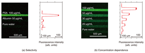
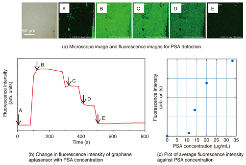
Aptamers have a wide variety of targets and offer many advantages as molecular recognition probes. Aptasensors are generally versatile because they can be extended to the detection of many different targets by replacing the aptamers. We confirmed the versatility of our on-chip graphene aptasensor by using it to detect three different proteins, namely, thrombin (a blood clotting marker), prostate specific antigen (PSA; a cancer marker), and hemagglutinin (an antigenic glycoprotein found on the surface of influenza viruses), simply by changing the aptamers but retaining the same sensor composition. Moreover, aptamers can be flexibly designed without loss of bioactivity. Thus, we can design and construct various kinds of biomolecular probes by conjugating additional functions with an aptamer. Lastly, aptamers are chemically stable. We confirmed that the aptasensors that had been stored at a normal temperature and pressure for more than a month operated normally as if they had just been made. 3. Multichannel configuration for quantitative detection and linear-array for multiple protein detectionWe first studied the sensing performance of our aptasensor by using GO and confirmed their usefulness for protein detection. An advantage of using an on-chip sensor is that it enables us to realize a parallel analysis system such as a sensor array. A multichannel system allows us to make a precise quantitative sample-reference comparison. It also enables us to perform simultaneous observations of the sample and reference signals, which can be used to eliminate the effect of fluorescence degradation caused by laser exposure and other noises. This is an advantage of our on-chip graphene aptasensor. Moreover, the on-chip aptasensor requires no out-of-chip processes such as labeling or mixing the sample, and thus, the human errors that can occur during the sample preparation procedure can be minimized. We fabricated an on-chip multichannel aptasensor by placing a polydimethylsiloxane sheet with microchannels on a solid substrate, and we formed the graphene aptasensor on its surface. The target protein was detected in about a minute simply by adding a sample solution smaller than 1 microliter to the sensor chip. We measured the fluorescence emitted from the graphene surfaces located in each microchannel simultaneously and compared the intensities of the channels. For comparison, a commercially obtained ELISA (enzyme-linked immunosorbent assay) kit—one of the most common protein detection methods—requires a sample volume of at least 100 microliters and an assay time of three hours. We can fabricate a microchannel with the desired design using photolithographic techniques. The number of channels is also variable. Here we prepared an on-chip aptasensor with a triple microchannel configuration. We measured the fluorescence images when PSA, human albumin solution, and water were injected into the top, middle, and bottom channels, respectively (Fig. 2(a)). Albumin, the most abundant protein in human blood plasma, caused no change in the fluorescence intensity, just as with water. This proved the selectivity of our aptasensor for PSA detection. We also examined the dependence of the fluorescence intensity on the PSA concentration (Fig. 2(b)). We used a quintuple microchannel configuration and injected PSA solution with four different concentrations and water as a reference into each microchannel. The results showed that the fluorescence intensity became weaker as the PSA concentration decreased.
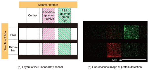
We fabricated a 2×3 linear-array aptasensor by using two different aptamers for different targets, namely thrombin and PSA, which we labeled with red and green fluorescent dyes, respectively (Fig. 3(a)). Bright fluorescence was only observed in the areas where we assumed that the correct aptamer-target pair had been formed (Fig. 3(b)). The simultaneous detection of multiple target molecules on a single chip was successfully demonstrated [4].
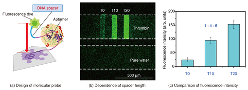
4. Molecular design for enhanced sensitivityThe most interesting feature of aptasensors is that we can design and construct various kinds of biomolecular probes by incorporating additional functions with an aptamer. We can improve the sensitivity of an on-chip GO aptasensor by modifying an aptamer with an ssDNA spacer (Fig. 4(a)). The strategy was to increase the distance between the fluorescence dye and the graphene surface, which is crucial for FRET-based sensors, when forming a complex with the target protein. We fabricated a 2×3 linear-array GO aptasensor by using three different probes and introducing ssDNA spacers with 0, 10, and 20 thymine segments between the aptamer and the dye. The fluorescence intensity increased significantly with increases in the spacer length (Figs. 4(b) and 4(c)). The limit for thrombin detection was about 1 nM, which corresponds to the in vivo concentration range during blood clotting by using the probe with 20 thymine segments, the best design in our present study. The results showed that introducing an ssDNA spacer at the correct position is an effective way of enhancing sensor sensitivity [5, 6].
5. Aptasensor built on continuous single-layer graphene surfaceIn our GO aptasensor, we used a pyrene linker that showed a strong affinity with the graphene-like domain to immobilize the aptamer. However, the surface area of the graphene-like domain reached at most 50% that of a GO flake. By changing the platform from GO to graphene, we were able to achieve a solid surface with a 100% graphene structure. We prepared a PSA aptasensor on a commercially available single-layer graphene surface fixed on a solid substrate. We confirmed that the substrate was almost fully covered with a single layer of graphene by observing optical and Raman images before measuring the sensing performance. The fluorescence intensity was initially small (Figs. 5(a) and 5(b), A), increased steeply after PSA was added (B), and then decreased rapidly as water was added to dilute the sample solution (C - E). It is noteworthy that the fluorescence intensity was almost homogeneous in the observed area of more than 100 µm × 100 µm. The maximum fluorescence intensity was larger than that of a GO aptasensor prepared in the same manner; namely, the ratio reaches 3.3. Thus, we can improve the sensitivity by changing the sensing platform from GO to graphene. An investigation of the mechanism behind the improvement in sensitivity is ongoing [7].
References
|
||||||||||||||||