|
|||||||||||
|
|
|||||||||||
|
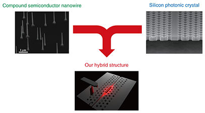
Feature Articles: Forefront of Research on Integrated Nanophotonics Vol. 16, No. 7, pp. 20–25, July 2018. https://doi.org/10.53829/ntr201807fa4 Compound Semiconductor Nanowire Laser Integrated in Silicon Photonic CrystalAbstractCompound semiconductor nanowires were integrated in silicon photonic crystals to form nano-cavities in arbitrary places, achieving the first nanowire laser that oscillates continuously at communication wavelengths. High-speed modulation at 10 Gbit/s was demonstrated. This laser is the ultimate heterostructure material hybrid device, having gain material only within the cavity. Keywords: photonic crystal, nanowire, nanolaser  1. Fusion of heteromaterials with nanophotonicsThe integration of compound semiconductors on silicon is very important for optoelectronic devices for optical interconnection, optical computing, and on-chip devices. Wafer bonding is generally used to bond compound semiconductors and silicon, which are dissimilar materials. Although that method enables the integration of heteromaterials such as compound semiconductors on silicon, it involves problems such as the difficulty of bonding and the difficulty of obtaining the utmost optical function of the optical elements, which themselves are compounds, due to overheating. In our work, we have adopted a configuration in which high-performance optical elements made of optically low-loss silicon are prepared and compound semiconductor nanowires are placed as gain parts in the necessary locations. This fabrication process does not involve heating, so damage due to overheating does not occur. Moreover, the optical loss is low because the device is based on silicon. Another advantage is that the environmental impact is very low because there is minimal use of the compound semiconductor. Accordingly, this device can be considered an ideal heteromaterial hybrid optical device. The device described here is a new nanolaser with a hybrid structure comprising silicon photonic crystal and a compound semiconductor. The nanowire is a one-dimensional structure that can be fabricated on a substrate in large numbers at one time. The nanowire can serve various purposes, including a quantum well, quantum dot, and p-i-n (p-type, intrinsic, n-type semiconductors) junction, which can be controlled by switching the gas that is supplied during growth. However, the nanowires themselves are too small to efficiently provide strong light confinement. Silicon photonic crystal, on the other hand, can provide very efficient light confinement without optical loss, but silicon is an indirect transition semiconductor and cannot itself emit light. In our work, we fabricated a nanolaser by introducing an indium arsenic phosphide and indium phosphide (InAsP/InP) nanowire quantum well into a silicon photonic crystal to form a micro-cavity (Fig. 1). This combination can be considered a landmark structure that compensates the weak light confinement of the nanowire and the absence of light emission by the photonic crystal with the light emission of the nanowire and optical confinement of the photonic crystal. This type of structure was used to demonstrate the world’s first nanowire laser that operates continuously in the communication wavelength band [1].
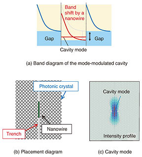
2. Fabrication of hybrid nanowire devicesThis device is fabricated by transferring nanowires onto a silicon substrate and then moving them onto the photonic crystal with the probe of an atomic force microscope (AFM)*1 [2]. This method makes it possible to place any nanomaterial freely on a photonic crystal or other optical circuit. The nanowires used here were fabricated by the VLS (vapor-liquid-solid) method using metal-organic vapor phase deposition [3]. The InP nanowires are grown from gold particles 40 nm in diameter that are dispersed on an InP (111) B substrate. One hundred InAsP layers are formed internally by supplying arsenic for a short time during the nanowire growth. The light emission characteristic of the nanowire quantum well has a spectrum peak in the 1.3-µm band, and the polarization direction of the emitted light is controlled to be perpendicular to the nanowires. The nanowires are 2.4-µm long and have an average diameter of 114 nm (82 nm minimum and 144 maximum). The silicon photonic crystal has a diameter of 200 nm, a lattice constant of 370 nm, a trench width of 150 nm, and a depth of 115 nm. The nanowires are placed in grooves in the prefabricated photonic crystal. The photonic band at the location where the nanowires are placed is shifted towards shorter wavelengths, and the optical characteristics are changed only at those locations. Because light of particular wavelengths is confined in those locations, cavities are formed. Such photonic crystal cavities are called mode gap cavities (Fig. 2(a)). The polarization of the cavity mode is consistent with the polarization of the nanowire itself, so light can be extracted efficiently. From simulations of the light intensity when nanowires are placed in the photonic crystal (Fig. 2(b) and (c)), we can see clearly that oscillators are formed, and light is strongly confined at the nanowire locations. Because cavities are formed in the optical waveguide by simple placement of nanowires, this is a very convenient structure.
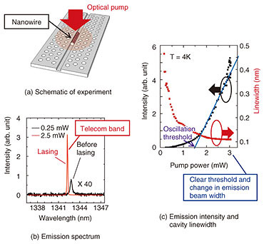
3. Nanowire laserNext, we investigated the oscillation of the laser produced by the nanowires. A conceptual diagram of the measurement and the measured spectra before and after oscillation produced by placement of the nanowires on a photonic crystal are presented in Fig. 3(a) and (b). Light emission was measured using the microscopic photoluminescence method. The device was illuminated with light to excite the nanowires, and the light emitted by the nanowires was measured with a detector. The specimen was cooled to a temperature of 4K. The emission spectrum is steep, as seen in Fig. 3(b). That is the spectrum of the nano-oscillator induced in the photonic crystal by the nanowire. Furthermore, when the excitation power is high, the laser oscillates with sharp increases in emission intensity. We investigated this effect in detail by measuring the nanowire emission while varying the excitation power (Fig. 3(c)) (light-in, light-out (L-L) measurement). The dependence of the emission and the spectral linewidth of the cavity on the excitation strength is shown in the figure. Generally, the emission sharply increases, and the cavity spectrum width becomes narrow when the laser oscillates, and the result presented here exhibits that behavior. The emission becomes strong at the excitation power of 0.15 mW (the oscillation threshold of the laser), confirming laser oscillation with certainty.
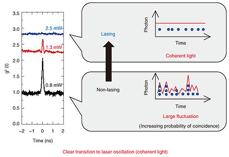
Oscillation of the laser can also be confirmed by investigating photon statistics. Correlation measurements can be used to investigate the time intervals between photons. The light prior to laser oscillation is called spontaneous emission light and is characterized by a large variance in intensity with short time intervals between photons (referred to as bunching because the photons are close together). The light after laser oscillation, on the other hand, is called coherent light, because the intensity is stable and there is a uniform distribution of the intervals between photons. The measurements require detection of a photon-level signal, so we used a highly sensitive superconducting single-photon detector*2 to determine the correlation function (g2(t)). Prior to oscillation, the correlation for this function is at t = 0, and bunching is observed (g2(0) > 1). However, that bunching signal is eliminated once the laser oscillation begins. The effect of change in the excitation power on g2(t) is that the bunching signal is eliminated and the laser transition occurs (Fig. 4). Laser oscillation is confirmed to continue after that point.
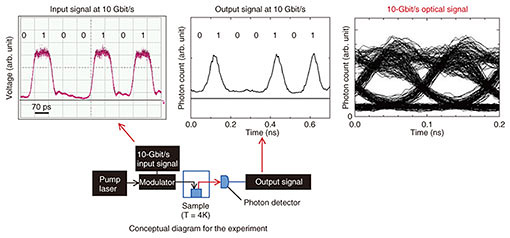
Next, we conducted communication experiments with bit signals produced by this laser. The conceptual diagram for the experiment and the input signal, output signal, and eye diagram are presented in Fig. 5. The input signal was a 10-Gbit/s pseudorandom pattern produced by a pulse pattern generator. The input light was modulated by an electro-optic modulator, and the signal output from the nanolaser was integrated by the superconducting single-photon detector for measurement. Normally, a sampling oscilloscope and photodetector are used for measurement, but the extremely weak light emitted by the nanolaser is measured in free space, so a highly sensitive detector is used. The light used for excitation has sufficient power to produce laser oscillation. We can see that the obtained waveform is the same as the waveform of the input signal. We analyzed the signal to obtain an eye diagram. The open center of the eye pattern indicates that correct communication of the bit signal is possible.
4. Future developmentWe achieved continuous-wave laser oscillation at communication wavelengths by introducing compound semiconductor nanowires into silicon photonic crystals. We also confirmed that laser oscillation can be evaluated with photon statistics as well as with L-L characteristics. We further confirmed that the laser can be modulated directly at about 10 Gbit/s by modulating the excitation light with a pseudorandom signal. This demonstration of a communication-band nanowire laser and confirmation of modulated operation of a single nanowire laser are world-first achievements. While the demonstration described here was performed at low temperature, we are aiming for room-temperature operation in the future. The current nanowires and optical confinement are insufficient. Improvement will require thicker nanowires and control of non-emissive re-coupling at the nanowire surface. The structure of the photonic crystal should also be considered. We also plan to fabricate a current injection structure by using nanowires that have a p-i-n structure. In the future, we plan to develop new on-chip devices through on-chip integration of current-injected nanowire lasers, nanowire optical detectors, and nanowire optical modulators. References
|
|||||||||||