|
|||||||||
|
|
|||||||||
       |
Feature Articles: Creating Novel Functional Materials Vol. 17, No. 10, pp. 24–29, Oct. 2019. https://doi.org/10.53829/ntr201910fa5 High-quality Atomic-layer Materials Fabricated by Chemical Vapor DepositionAbstractAtomic-layer materials such as graphene and hexagonal boron nitride (h-BN) are promising for their use in next-generation optoelectronic devices due to the novel and unique physical phenomena as well as superior material properties being demonstrated in such materials. Scalable fabrication methods for high-quality atomic-layer materials are essential for their industrial applications. We introduce here chemical vapor deposition growth for high-quality graphene and h-BN. Keywords: atomic-layer materials, chemical vapor deposition, crystal orientation control
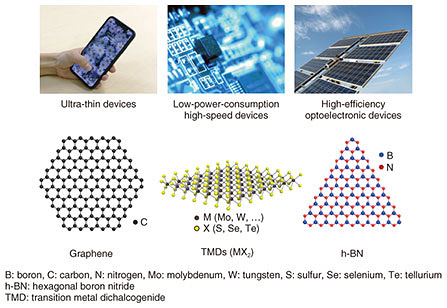
1. Atomic-layer materialsAtomic-layer materials have layered structures with a thickness of only one or a few atoms (Fig. 1). Graphene, a representative atomic-layer material, consists of a single layer of carbon (C) atoms arranged in a two-dimensional hexagonal lattice structure like a honeycomb, and is therefore an extremely thin material with a thickness of only one atom [1]. Graphene shows a semimetallic (or zero-gap semiconductor) character with a linearly dispersed energy band, which results in high carrier mobility (electrical conductivity) and large wavelength-independent light absorption in a wide range from infrared to visible light. Furthermore, graphene has the highest thermal conductivity and mechanical strength of any kind of material.
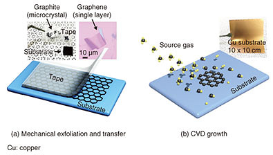
In addition to graphene, there are many kinds of atomic-layer materials including transition metal dichalcogenides (TMDs), MX2 (where M is a transition metal atom such as Mo (molybdenum) or W (tungsten), and X is a chalcogen atom such as S (sulfur), Se (selenium), or Te (tellurium). Hexagonal boron nitride (h-BN) is another type of atomic-layer material. Monolayer TMDs consist of a single layer of transition metal atoms (M) sandwiched between two layers of chalcogen atoms (X); thus, the total thickness is three atoms. Some TMDs are semiconductors with bandgaps in the near-infrared to visible spectral region, and the bandgap energy varies with the number of stacked layers. TMDs have also unique properties such as spin- and valley-dependent electrical and optical properties. The material h-BN is composed of boron (B) and nitrogen (N) and has a layered hexagonal lattice structure similar to graphene. h-BN is an insulator with a large band gap of about 6 eV and is therefore used as an insulating layer and a tunnel barrier in various types of devices made from atomic-layer materials. There are numerous atomic-layer materials ranging from metallic, superconducting, magnetic, semiconducting, to dielectric or insulating depending on their chemical composition and crystal structure, which means they are promising for next-generation devices such as ultra-thin flexible, low-power-consumption, high-speed nanoelectronic, high-efficiency photonic, and high-sensitivity devices. Thus, the application of atomic-layer materials will lead to innovative information technology. 2. Fabrication of atomic-layer materialsVarious fabrication methods for atomic-layer materials including mechanical exfoliation and thin-film growth are proposed. In mechanical exfoliation, a monolayer flake is cleaved from a microcrystal by using adhesive tape and is transferred onto a substrate, as shown in Fig. 2. K. S. Novoselov and A. K. Geim, Nobel laureates in Physics in 2010, demonstrated mechanical exfoliation for graphene and showed new phenomena in quantum physics. Mechanical exfoliation has been used in fabricating atomic-layer materials in order to investigate their physical properties and to demonstrate new functional device applications. However, the size of the atomic-layer material obtained with this method is limited to the size of the microcrystals, typically about tens of micrometers (μm). This small size is not suitable for industrial applications.
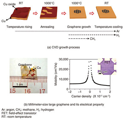
Chemical vapor deposition (CVD) is a growth method for thin films on large-area wafers (substrates) via chemical reaction of gas sources. It is widely used in the semiconductor industry for mass production of thin films. CVD growth technology is currently under development all over the world for atomic-layer materials. Although CVD growth of atomic-layer materials on large-area substrates has been demonstrated, the crystal quality is low, mainly due to defects originating at the boundaries of randomly orientated domains. The domain size is as small as tens of micrometers, similar to that of mechanically exfoliated flakes. In this article, we introduce our CVD technology for large-area single-domain graphene and for crystal orientation control of h-BN. 3. Large-size single-crystal graphene growthA schematic diagram of CVD growth of graphene on a copper (Cu) substrate is shown in Fig. 3(a). The surface of as-received Cu is naturally oxidized. In a CVD reactor, the Cu substrate is heated to the growth temperature at ~1000°C and thermally annealed under argon (Ar) and/or hydrogen (H2) flow to remove the natural oxide layer on the Cu surface. Then methane (CH4) is introduced for graphene growth. When the growth starts, graphene domains (nuclei) form on the Cu surface. The domain size increases with growth time. Once the domains coalesce with nearby domains, the graphene covers the entire Cu surface. Note that the lower nucleation density results in a larger domain size. After the growth, CH4 is shut off and the sample is cooled to room temperature. The domain size can be controlled by the nucleation density, which depends on CVD growth conditions, the substrate material, and its surface condition. Regarding the surface conditions, the Cu oxide prevents the nucleation of graphene while graphene preferentially nucleates on the clean Cu surface without the oxide. In the thermal annealing of the substrate, the etching rate of the oxide layer depends on the ambient gas. For example, the etching rate of the Cu oxide under H2 gas is higher than under Ar gas. To vary the coverage of the oxide layer for nucleation density control, we carried out thermal annealing of the Cu substrate under Ar gas alone and precisely adjusted the annealing time as shown in Fig. 3(a). Consequently, we succeeded in fabricating a millimeter-size graphene single crystal that is about 100 times larger than conventional ones with domain sizes of approximately tens of micrometers [2] (Fig. 3(b)).
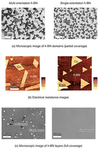
Next, we fabricated field-effect transistors in order to characterize the electrical properties of the graphene. The millimeter-size graphene showed nearly 10 times higher charge mobility than conventional CVD-grown ones. These results show that nucleation control by selective growth is a promising way to achieve large-area growth of high-quality graphene single crystals. 4. Crystal orientation control of h-BNSimilar to graphene, h-BN can be grown on Cu substrates by CVD. For h-BN growth, ammonia borane (H6BN) was used as a BN source. The crystal orientation of thin-film materials generally depends on the surface structure and symmetry of the substrate. Cu has a face-centered cubic lattice structure. For example, on Cu (001), (101), and (111) planes, h-BN shows multiple orientations, that is, two or four orientations due to the crystal rotational symmetry mismatching between h-BN and Cu. The multiple orientations cause crystal defects formed at the boundaries of domains with different orientations (rotation angles). The commercial Cu substrate is polycrystalline. During the thermal annealing process, the Cu substrate is recrystallized by heating. In recrystallization, polycrystalline grains coalesce and become large, and specific crystal planes of the grains appear on the substrate surface. We systematically investigated the crystal orientation of h-BN domains grown on more than 100 different Cu crystal planes. For h-BN grown on crystal planes inclined from a Cu (101) plane, as shown in the microscopic image (Fig. 4(a)), we found that all of the triangular h-BN domains are oriented to the same direction, indicating the formation of single-orientation h-BN [3]. We clarified the mechanisms of the single-orientation h-BN formation using theoretical calculations. In the case of a (101) plane, there are two energetically stable orientations for h-BN because the (101) plane has two-fold rotational symmetry. In contrast, for the inclined (101) plane, because the symmetry is broken, there is only one energetically stable orientation for h-BN, resulting in single-orientation h-BN formation. This mechanism is applicable to other atomic-layer materials. To investigate the effect of the crystal orientation on the electrical properties, we measured the electrical resistance images of the multi- and single-orientation h-BN as shown in Fig. 4(b). The single-orientation h-BN showed higher electrical resistance (darker contrast) than multi-orientation h-BN. This is because the single-orientation h-BN has lower defect density than multi-orientation h-BN. Finally, we grew h-BN layers that fully covered the Cu substrate as shown in Fig. 4(c). For the multi-orientation h-BN, multi-layer h-BN domains were partly formed on single-layer h-BN. In the case of the single-orientation h-BN on the other hand, no multi-layer h-BN domains were formed, and single-layer h-BN was uniformly formed on the entire Cu surface. Thus, the single-orientation control is essential to achieve high-quality atomic-layer materials.
5. Future prospectsCVD growth of heterostructures for a variety of atomic-layer materials is a challenging process to realize novel functional devices. Vertical heterostructures, in which atomic-layer materials are stacked, have demonstrated recently that material properties change greatly depending on the crystal orientation (rotation angle) of each layer. Furthermore, lateral heterostructures, in which different atomic-layer materials are atomically bonded in-plane, can lead to new physical phenomena originating from one-dimensional heterointerfaces and in-plane superlattice structures. We will continue to develop CVD growth technologies for high-quality heterostructures on large-area substrates for integrated functional devices. References
|
||||||||