|
|||||||||||||||||||||||||||||||||||||
|
|
|||||||||||||||||||||||||||||||||||||
       |
Feature Articles: Front-line Research on Graphene Vol. 11, No. 8, pp. 5–9, Aug. 2013. https://doi.org/10.53829/ntr201308fa1 Graphene Research at NTTAbstractGraphene, a two-dimensional sheet of carbon atoms, was experimentally discovered in 2004. Since then, graphene research has progressed exponentially from basic science to applications. NTT aims to make a large impact on the information society through the materials science of graphene and is therefore promoting a wide range of graphene research projects from theory to devices. In this Feature Article, the current status of graphene research underway at NTT laboratories is presented.
1. IntroductionHistorically, the development of new materials has revolutionized our way of life, and we have learned that an infinite variety of materials can be formed from different combinations of atoms and molecules. Research on materials science increases our knowledge of how to create and develop new materials and therefore has great potential for improving our lives and society. NTT laboratories have already created various new materials that have had a significant impact on the information society and are continuing to search for materials that will contribute to solving social issues in the future. These Feature Articles focus on graphene, which is currently attracting a great deal of attention both at a fundamental level and in technological domains. NTT laboratories are approaching graphene multilaterally from various aspects: theory, synthesis, physical properties, and devices. In this article, I first explain why graphene is such a promising material and then present an overview of graphene research at NTT. 2. Graphene2.1 Basic structureGraphene is a two-dimensional crystal consisting of carbon atoms arranged in a honeycomb lattice (Fig. 1). A three-dimensional stack of graphene sheets is graphite, which is a familiar material in daily life. Graphene is also the basic element of fullerenes and carbon nanotubes, which are well-known carbon nanostructures. However, its experimental history is relatively new. Researchers from the University of Manchester first discovered graphene in 2004 when they managed to isolate it from thin graphite flakes that had been mechanically exfoliated from bulk graphite. It has been researched intensively ever since, owing to its novelty in science and the expectations of its having a wide range of applications. The Nobel Prize in Physics was awarded to the discoverers in 2010.
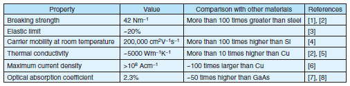
The scientific novelty of graphene is symbolized by its extraordinary electronic structure. Since the equation that describes the states of conduction electrons in graphene is the same as the relativistic quantum mechanical equation (Dirac equation) with mass equal to zero, conduction electrons in graphene are called massless Dirac particles. These electrons constitute a new class of two-dimensional electron system, which is truly different from the two-dimensional electron gas in semiconductors such as silicon (Si) and gallium arsenide (GaAs). For example, the energy of electrons is normally proportional to the square of the momentum, but the energy of conduction electrons in graphene is proportional to the momentum. This property is the same as that of light and is compatible with massless particles. 2.2 Properties and synthesisGraphene has excellent mechanical, electrical, and optical properties. Its typical properties are summarized in Table 1. Graphene is mechanically very strong and flexible. The breaking strength of graphene is more than 100 times greater than that of steel. The crystal structure does not break even after being stretched up to 20%. From an electrical aspect, the carrier mobility of graphene at room temperature is more than 100 times higher than that of silicon. Furthermore, graphene is an ultra-wide-band optical material that interacts strongly with light of a wide range of wavelengths. Graphene absorbs 2.3% of light in the visible to infrared region. This absorption coefficient is one to three orders of magnitude higher than those of conventional semiconductor materials.
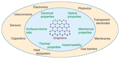
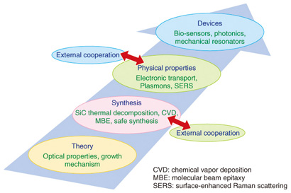
These properties of graphene suggest that various applications are possible. For example, several-layer-thick graphene films are transparent, electrically conductive, and flexible. Therefore, flexible transparent electrode applications, including touch screens and solar cells, have been extensively studied. High carrier mobility makes graphene promising as a channel material of high-speed electronics. However, since it is difficult to turn off an electrical current in graphene, progress has mainly been achieved in research on applications involving analog high-frequency devices. Graphene is also promising for photonics devices such as modulators and photodetectors. In general, the range of potential applications is very wide and includes sensors, interconnects, capacitors, heat dissipaters, gas barriers, and membranes. High-quality graphene can be obtained by mechanically exfoliating graphene from graphite. This method is therefore ideal for basic research, but in terms of productivity and the small size of graphene sheets that can be obtained, it is not suitable for industrial applications. Therefore, in recent years, techniques for growing graphene on a substrate have been actively studied. Two growth methods are attracting intense interest: thermal decomposition of silicon carbide (SiC), in order to grow graphene on it, and chemical vapor deposition (CVD) to grow graphene on metal catalyst substrates. The quality of the graphene grown using these methods is improving rapidly. If single-crystal graphene substrates could be obtained routinely, they would dramatically advance graphene research and increase the number of potential applications. 3. Graphene research at NTTNTT has a comprehensive research scope ranging from basic theory to applied research, and we are studying graphene across this entire spectrum. Further, to accelerate the research in order to elucidate graphene’s fundamental properties and its synthesis, we are actively collaborating with research institutes outside NTT. Typical research topics in four research stages: theory, synthesis, physical properties, and devices are shown in Fig. 2.
3.1 TheoryThe Feature Article in this issue entitled “Basic Principles of Raman Spectroscopy for Graphene” [9] covers the theory of the optical properties of graphene. Another important research subject is the theory of graphene growth. On the basis of our understanding of the stable structures of carbon atoms on SiC determined from first principles calculations*1, we are trying to clarify the mechanism of graphene growth by thermal decomposition of SiC. 3.2 SynthesisNTT possesses a low-energy electron microscope (LEEM)*2 that is suitable for in-situ observation of the graphene growth process and for microscopic evaluation of the number of graphene layers. We used LEEM to investigate the growth process of graphene on SiC, and from the insights gained, we succeeded in growing highly uniform monolayer and bilayer graphene. These graphene substrates enabled us to evaluate the electronic transport properties at each thickness, as introduced in the Feature Article entitled “Exploring Relativistic Physics and Band Gap Detection in Epitaxial Graphene” [10]. NTT laboratories are working on growing not only graphene but also monolayer boron nitride (BN), a two-dimensional crystal consisting of boron and nitrogen, using CVD. In particular, we are promoting external cooperation with the aim of establishing a technique for growing single-crystal graphene and BN by using single-crystal metal thin films on a sapphire substrate. In addition to the results obtained in CVD and thermal decomposition of SiC, we have achieved many promising results in graphene and BN synthesis, as exemplified by a safe synthesis method that uses a solid material deposited on a metal substrate as a source, which is presented in the Feature Article entitled “A Novel and Simple Method of Growing Atomically Thin Hexagonal Boron Nitride” [11], and by the direct growth of graphene by molecular beam epitaxy (MBE)*3. 3.3 Physical propertiesThe Feature Articles entitled “Exploring Relativistic Physics and Detection of a Band Gap in Epitaxial Graphene” [10], “Plasmon Transport in Graphene” [12], and “Surface-enhanced Raman Scattering of Graphene on SiC” [13] report that NTT laboratories have obtained many notable results on the optical and electronic properties of graphene. Further, because the electronic transport properties of graphene grown on SiC are influenced by the substrate, we are also attempting to control the interface structure to improve the transport properties. In addition, we are working to clarify the fundamental physics of graphene by promoting collaboration with external research institutions that apply unique characterization methods such as high-sensitivity measurements of polarization rotation of terahertz waves and magneto-optical absorption measurements under an ultra-high magnetic field. 3.4 DevicesThe Feature Article entitled “Biosensing on a Graphene Oxide Surface” [14] explains how graphene oxide produced by chemical oxidation and exfoliation of graphite can be used for protein detection. NTT laboratories are also investigating the vibration characteristics of mechanical resonators fabricated from graphene grown on SiC by electrochemically etching the substrate, and exploring the light transmission characteristics of optical waveguides integrated with graphene.
4. Future prospectsThere is no doubt that graphene has enormous potential as a future material, but we face many challenges in achieving industrial applications. The synthesis method is a prime example. The CVD method is suitable for large-scale and low-cost synthesis of graphene, but electronics/photonics applications require that graphene on metal substrates be transferred onto other insulating substrates. Damage-free transfer technology is also a difficult challenge. Further, the ideal graphene does not have a band gap, which impedes the development of logic devices. In these Feature Articles, we will describe the electrical detection of a band gap in bilayer graphene on SiC. Various attempts to create a band gap in graphene have been made from materials science and device science approaches. On the other hand, the discovery of graphene has aroused increasing interest in two-dimensional crystals other than graphene, such as insulating BN and semiconducting molybdenum disulfide (MoS2). It is expected that hybrid structures of two-dimensional materials with various properties will bring new functions. Although research on two-dimensional crystals containing graphene is very competitive, we are confident that NTT laboratories, with NTT’s comprehensive research organization and research network outside NTT, will be at the center of graphene research and will attain new levels of understanding that will contribute to our society. References
|
||||||||||||||||||||||||||||||||||||