|
|||||||||||||||||||||
|
|
|||||||||||||||||||||
       |
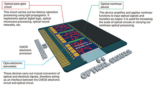
Feature Articles: Photonics-electronics Convergence Technology to Achieve All-Photonics Network Vol. 18, No. 10, pp. 31–37, Oct. 2020. https://doi.org/10.53829/ntr202010fa4 Nanophotonic Technologies toward Opto-electronic Integrated AcceleratorsAbstractThe opto-electronic integration technology being researched at the NTT Nanophotonics Center is for creating a photonic computing platform with low latency and low energy consumption. The development of miniature optical functional devices through nanophotonics along with advances in large-scale optical-circuit fabrication technology will make diverse types of photonic-information processing possible. This article introduces the technologies that we are researching for optical pass-gate circuits, opto-electronic converters, and optical nonlinear devices and presents the path to opto-electronic integrated accelerators that the combined use of these technologies will make possible. Keywords: opto-electronic integration, photonic computing, photonic crystal
1. Optical technology: from communication to processingOptical technology is currently the driving force behind large-capacity information transmission including long-haul optical fiber communication and inter-server communication in datacenters. By extension, progress in optical communication for shorter distances can be considered but will ultimately mean optical networking on a computer chip and information processing based directly on light. Developing an optical computer has been one of the major goals of researchers in the field of optics, but the mature complementary metal-oxide semiconductor (CMOS) electronic circuit technology has prevented any meaning from being found in using light in computing. However, CMOS-based nano-fabrication and circuit integration are gradually approaching their limits, so expectations are increasing for information processing using the high-speed properties of light [1]. These expectations are being boosted by progress in miniature and energy-saving optical device and circuit technology made possible by fine-processing technology called nanophotonics. Recent advances in silicon photonics technology are also generating strong synergy with nanophotonics, and the implementation of a large-scale optical circuit in a compact space is expanding the opportunities for photonic computing research. Though it is generally difficult to carry out various types of information processing solely with optical circuits, importance is being given to an accelerator that can accelerate specific processing by combining optical circuits with the parallel digital processor and large-capacity memory of CMOS electronics and enabling optical circuits to carry out high-speed-specific processing applicable to light [2]. In particular, the value of using light has been reevaluated recently as extending beyond digital processing to include analog processing as in machine learning and photonic microwave-signal processing, and an opto-electronic integrated accelerator that links CMOS electronics and nanophotonics has begun to take form. The following introduces a low-latency optical pass-gate circuit, opto-electronic converters, and an optical nonlinear device as three key components deemed essential to developing an opto-electronic integrated accelerator (Fig. 1).
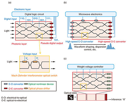
2. Low-latency optical pass-gate circuitThe barrier to the continuation of Moore’s law in CMOS electronic circuits (empirical rule stating that performance improves due to finer processing and greater integration) is the increase in signal delay and heat generation as a result of resistance and capacitance of transistors and metal wiring. In electronic circuits, digital logic operations, such as AND-OR-INVERT logic, are carried out by cascaded connection of logic gates. A subsequent gate waits for the signal output from a prior gate so that the time delay to obtain the calculation result increases proportionally to the number of gate stages. In addition, increasing the signal bit rate increases heat generation due to an increase in the movement of free electrons in metal. As a consequence, the signal bit rate of CMOS electronics for computing that requires low power consumption has generally been held to several gigahertz. For these reasons, the current situation is that, while processing capacity (throughput) can be increased through further increases in CMOS fine processing and integration, processing delay (latency) is hitting a ceiling. As shown in Fig. 2, an optical pass-gate circuit consists of the integration of optical switches that switch optical transmission paths. In the example shown in Fig. 2(a), calculation results are output by triggering Mach-Zehnder interferometer optical switches* at the same time by signals from the electronic circuit and transmitting light along the selected paths as light beams interfere with each other. There is no power loss or heat generation due to resistance, as in the case of electronic circuits, and calculations are carried out through the interference of light, which opens the door to low-energy and low-latency processing. We can take as an example a full-adder circuit that inputs digital signals (“1” and “0” binary signals). The calculation of the carry signal from least-significant bit to most-significant bit constitutes the adder’s critical path that determines total delay. However, carrying out such processing using optical pass-gates is expected to reduce delay compared with that of electronic circuits [3]. Therefore, optical pass-gates should be applicable to other digital operations including basic arithmetic operations.
In addition to digital processing, progress is also being made in analog processing (carried out with continuous values). In particular, there are high expectations for microwave photonics technology to convert microwave signals used in wireless communications to light, execute processing that requires high spectral resolution and temporal resolution (filtering, waveform control, dispersion control, etc.) in the optical domain, and output the results again as microwave signals (Fig. 2(b)) [4]. At the same time, research on optical neural networks is becoming quite active worldwide along with advances in deep learning and other artificial intelligence technologies. At the core of this analog processing is vector-matrix multiplication (VMM), but its calculation cost has been a bottleneck in CMOS digital circuits. On the other hand, a pass-gate circuit based on light interface can be used to physically implement VMM, so a solution to these problems is expected [5]. The possibility exists of achieving low-latency inference by combining this optical pass-gate circuit with an opto-electronic converter and optical nonlinear device, as described below, to configure opto-electronic neural network integration (Fig. 2(c)).
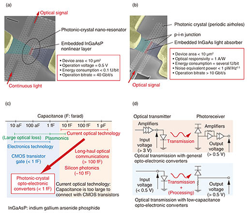
3. Opto-electronic converters (interface between optical and electronic circuits)A major issue in integrating CMOS and optical circuits is developing a high-density opto-electronic interface featuring a miniature and energy-saving electrical-to-optical (E-O) converter, i.e. an electro-optic modulator (EOM), and optical-to-electrical (O-E) converter, i.e. a photodetector (PD). We have been developing such converters using nanostructures called photonic crystals (Fig. 3), which are periodic structures formed in semiconductors. They can be used as ultrasmall optical waveguides and optical resonators by forming periodic airholes with diameters of ~200 nm on a thin semiconductor plate and arranging their layout. At NTT, we developed functional devices such as optical switches, optical memory, and laser sources and demonstrated record-low energy operation. We also demonstrated E-O and O-E converters, i.e., a nanophotonic EOM and PD, as shown in Figs. 3(a) and (b), and succeeded in dramatically reducing the size and energy consumption of these converters compared with those of conventional ones [6].
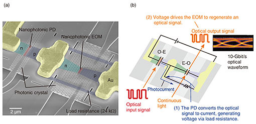
For E-O/O-E converters, the low electrical capacitance can be an important figure of merit. As shown in Fig. 3(c), the capacitance of a single CMOS transistor is less than one femtofarad (fF), whereas that of conventional E-O/O-E converters is generally large, i.e., 10 fF or greater. This requires high energy consumption in proportion to the large capacitance, creating a bottleneck. On the other hand, our converters can reduce capacitance to less than 1 fF, the same as that of CMOS transistors. Such a capacitance reduction is of major significance. As shown in Fig. 3(d), optical communication based on conventional E-O/O-E converters requires multiple amplifier stages to generate a sufficient voltage signal, which increases power consumption and device area. In contrast, the electrical energy required for logic operations in CMOS transistors can be sufficient to drive our low-capacitance converters, enabling seamless opto-electronic integration requiring no amplifiers. We therefore expect our converters to be used for configuring dense optical networks either between or within CMOS chips based on simple optical transceiver circuits with a strong energy-saving effect and for even optical-signal processing within communication. Going forward, the key to these advances is integrating CMOS and opto-electronic converters while maintaining low capacitance and developing opto-electronic interfaces toward practical computing applications. 4. Optical nonlinear device (optical transistor)Nonlinear operations such as signal switching and amplification, as in electrical transistors, play an important role in optical circuits. However, though light is particularly good at linear signal processing based on light interference, nonlinear signal processing generally requires strong light-matter interaction, which in turn requires high optical energy. To overcome this, we fabricated an O-E-O converter by integrating the nanophotonic PD and EOM described above, and developed an energy-saving optical nonlinear device (Fig. 4). The optical input signal to the PD is converted to current that is then converted to a voltage via load resistance (24 kΩ). This voltage, in turn, drives the EOM so that the input signal waveform is transferred to another light. This results in nonlinear signal transfer at 10 Gbit/s. With this operation, the optical output power from the EOM is at least two times greater than that of the optical input power at the PD. It can be said that we have achieved an optical transistor producing an optical signal gain in the same manner that an electrical transistor produces an electrical signal gain [7].
The electrical capacitance of this opto-electronic integrated device is extremely small at 2 fF, and such integration that maintains ultralow capacitance is the world’s first. Current O-E-O converters suffer from large capacitance, making energy consumption substantially high, but our low-capacitance device reduces this to several fJ/bit, which is less than 1/100 that of current devices. The fact that this device exhibits optical signal gain should enable multi-stage transfer of optical signals. Thus, it should be possible to connect and increase the scale of optical pass-gate circuits. We can also envision its applications including its use as a nonlinear optical neuron in the optical neural network shown in Fig. 2. 5. ConclusionThere are options to maximize the superior features of light and obtain a level of performance that exceeds that of electronic circuits. The ability of multiplexing optical information by wavelength, space, and time to increase the dimensions of processing provides a significant advantage over electronic processing. Practically, we need an opto-electronic co-design that takes into account opto-electronic converters, analog-to-digital converters, and the latency and energy efficiency within electronic circuits. An approximate computing design that balances accuracy and computing cost is becoming increasingly important [8]. Beyond the device technology (component level) introduced in this article, a broader perspective (architecture level) is required to discover the specific form that opto-electronic integrated computing should take. References
|
||||||||||||||||||||