 |
|||||||||||||||||||||||||||||||||
|
|
|||||||||||||||||||||||||||||||||
       |
Vol. 5, No. 9, pp. 4–11, Sept. 2007. https://doi.org/10.53829/ntr200709sp1 Crystal Growth and Electro-optic Properties of
|
||||||||||||||||||||||||||||||||

| † | NTT Photonics Laboratories Atsugi-shi, 243-0198 Japan. Email: tadayuki@aecl.ntt.co.jp |
|---|
1. Introduction
The electro-optic (EO) effect is a phenomenon in which the refractive index of a substance is modulated by an externally applied electric field. This phenomenon is used to make optical modulators where the intensity or phase of a light beam is modulated by an electric signal. Substances for which this phenomenon is significant are called electro-optic materials. The most common material is lithium niobate (LiNbO3, LN). For LN, the EO effect is linear; that is, the refractive index change is proportional to the applied electric field. This is called the Pockels effect. Potassium tantalate niobate (KTa1−xNbxO3, KTN) is another EO material that is well known because of the strength of its EO effect [1], [2]. The effect for KTN is quadratic (Kerr effect) where the refractive index change is proportional to the square of the electric field. Although the effects are different for these two materials, it is possible to compare their figures of merit by introducing a bias electric field. We can expect the EO effect to be more than ten times larger for KTN than for LN. To date, however, there have not been any commercial products utilizing KTN, while LN is already used in various products such as 40-Gbit/s light modulators for fiber-optic telecommunication in addition to surface acoustic wave filters for mobile phones. One important reason of this is that KTN crystal has been difficult to grow compared with LN. In 2003, our laboratories succeeded in growing sizable crystals of optical quality with volumes of over 30 cm3 (e.g., 40 mm × 40 mm × 20 mm) [3]. We recently improved the growth technique to achieve a high degree of reproducibility. Moreover, we additionally found that significant light beam deflection occurs in KTN single crystals [4], [5]. Promising beam deflection devices are expected to be developed by utilizing this new phenomenon.
In this paper, we introduce KTN crystal and its EO properties. Then, we review a growth technique called the top seeded solution growth method used for KTN single crystals [6]. We also present some examples of the EO properties of our crystals to show the high performance of KTN.
2. Potassium tantalate niobate
KTN is the mixture or solid solution of potassium niobate and potassium tantalate. Potassium niobate (KNbO3, KN) is also a well-known oxide crystal that is commonly used for optical second harmonic generation via its optical nonlinear effect. It is one of the perovskite-type materials whose general formula is ABO3. The crystallographic structure of perovskite is shown in Fig. 1. Cations of A are at the corners, cations of B go into the body center, and oxygen anions are at the face centers. The unit is drawn in a cubic shape in Fig. 1. In fact, it is cubic for KN crystals at high temperatures over 435°C. However, a KN crystal undergoes three phase transitions when cooling from such high temperatures, and its crystallographic structure changes. At the first transition, the cubic structure changes to a tetragonal structure. Next, it becomes orthorhombic, which is the phase at around room temperature. It then becomes rhombohedral at low temperatures. KN is regarded as a ferroelectric substance. It thus has spontaneous polarization with zero electric field. In the cubic phase, however, the spontaneous polarization vanishes and the crystal is paraelectric. Potassium tantalate (KTaO3, KT) is also a perovskite oxide. However, it does not undergo any phase transitions as the temperature changes but remains cubic. Therefore, the mixture KTN has three phase transitions like KN, but the transition temperatures change with the composition. All the transition temperatures rise as the KN fraction increases, as shown in Fig. 2 [1], [7].
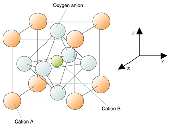
Fig. 1. Crystallographic structure of ABO3 perovskite.
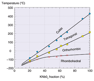
Fig. 2. Concentration dependence of the three transition temperatures for KTN.
KTN has a strong Kerr effect in the cubic phase, so it is usually used in the cubic phase. Suppose that a light beam propagates along the x direction in Fig. 1, the vibrating electric field of the light is parallel to the y direction, and a constant external electric field is applied also along the y direction. The resulting change in the refractive index caused by the external electric field is expressed as
![]()
where n0 is the original refractive index, E is the external field, and s11 is one of the Kerr coefficients. This s11 is given by [8]
![]()
where ε, ε0, and εr are the KTN permittivity, the vacuum permittivity, and the relative dielectric constant, respectively, and g11 is a function of the wavelength of the light but depends on neither εr nor the temperature. Because εr is much larger than 1 for KTN crystals, we can regard s11 as being proportional to εr2. According to the Curie-Weiss law, εr becomes significantly large at temperatures just above the phase transition temperature (the upper curve in Fig. 2. Hereinafter, the phase transition means the transition between the cubic and tetragonal phases and Tc means the temperature where this transition occurs). Therefore, we can obtain a huge Kerr coefficient s11 at room temperature by choosing the composition (KN fraction) so that Tc is around room temperature. We discuss the values of εr and s11 in section 4.
3. Crystal growth
It is essential to grow sizable single crystals with good optical homogeneity for EO oxide materials such as LN and KTN. KTN single crystals are grown by a method called top seeded solution growth (TSSG) [6], which is similar to the Czochralski method used for LN or silicon crystals. The growth apparatus for KTN single crystals is shown in Fig. 3. The furnace uses resistance heating elements. The mixed ingredients of the crystals are melted in the platinum crucible at temperatures such as 1200°C. We dip a seed crystal into the molten ingredients, slowly cool it, and thereby grow a crystal gradually from the seed. The seed crystal is attached to a rod that is simultaneously rotated and lifted by a mechanism located outside the furnace. This apparatus is almost the same as those used for Czochralski growth.
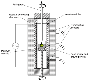
Fig. 3. TSSG apparatus for KTN single crystal growth.
However, KTN single crystals have been much more difficult to grow than conventional materials. This is mainly due to the fact that the grown crystals have different compositions from the molten ingredients. The phase diagram of the KT-KN system at elevated temperatures is shown in Fig. 4 to explain this situation [9]. The diagram shows two temperature curves as functions of composition, Tl (x) and Ts (x). Tl (x) is called the liquidus and Ts (x) the solidus. Above the liquidus, the substance is completely liquid. Below the solidus, the substance is solid. When we intend to grow a crystal from material with composition X0, we melt the material by heating it through the liquidus temperature T0 = Tl (X0). We then cool it to Tl (X0) and below. Here, the material is no longer completely liquid and solidification occurs. The composition of the solid (or crystal) is x0, which gives the same temperature T0 on the solidus Ts (x0). The KN fraction of the growing crystal is less than that of the liquid. Thus, niobium left over from the solidification is gradually concentrated in the liquid, especially near the growth interface. This concentration causes instability of the growth interface. Irregular growth is likely to occur in such a situation if the growth is too fast. Moreover, it is common to start the growth with a melt that contains additional potassium oxide with KTN ingredients because potassium oxide easily evaporates from the hot melt. Therefore, excess potassium also tends to be concentrated as the growth proceeds. As a result, single crystal growth of KTN is more difficult than that of conventional materials such as LN. The additional potassium oxide acts as a kind of solvent, and the melt is a solution. Therefore, the growth technique for KTN crystals is called the top seeded solution growth method.
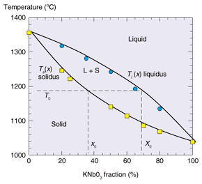
Fig. 4. Phase diagram at elevated temperatures to show the thermal equilibrium between the liquid and solid during the crystal growth.
The most noticeable defects in KTN crystals are inclusions containing excess potassium. They strongly scatter light beams and cause inhomogeneous variations in the refractive index around them. The main reason for the formation of the inclusions is excessive supercooling of the solution or excessively fast growth. We succeeded in suppressing the occurrence of inclusions by carefully controlling the furnace temperature and the growth speed [3]. We can now reproducibly grow sizable KTN crystals (> 30 cm3) without inclusions. A photograph of one of our crystals is shown in Fig. 5. The stump of the seed crystal can be seen on the center of the top face. Neither inclusions nor other irregular growths were observed. Sharp growth facets are often observed for crystals grown in furnaces with resistance heaters because of the gentle temperature gradient around the crucible. KTN crystals have a strong tendency to show crystallographic (001) faces [6]. Thus, it is possible to see through the mirror surface of the crystal in Fig. 5 even though we did not cut or polish it.
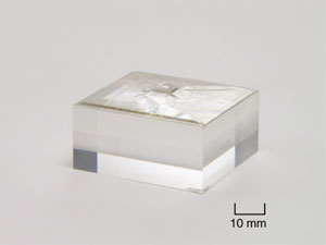
Fig. 5. Example of as-grown KTN single crystal.
4. Electro-optic properties
As described above, the relative dielectric constant of paraelectric KTN εr obeys the Curie-Weiss law:
![]()
Here, Tcp is the paraelectric Curie temperature. Thus, εr increases drastically as the temperature approaches Tcp. To obtain εr as a function of temperature, we cut a 6 mm × 5 mm × 1 mm chip from a grown single-crystal boule, polished its surfaces, formed a pair of platinum electrodes by evaporation, and measured its capacitance on a temperature-controlled aluminum block. The size of the electrodes was 5 mm × 1 mm and the gap between them was 1 mm. The applied voltage was 10 Vp-p AC with a frequency of 20 Hz. An example of the relative dielectric constant as a function of temperature is shown in Fig. 6(a). For this chip, the phase transition occurred at around 35°C. Above this phase transition temperature Tc, it was in the cubic phase. Below Tc, it was in the tetragonal phase. For this composition (or this Tc), it is known that the phase transition is of the first order and that Tcp is slightly lower than Tc. The reciprocal of the relative dielectric constant as a function of temperature is shown in Fig. 6(b). The 1/εr apparently obeyed the Curie-Weiss law (Eq. 3). It can also be seen in this figure that Tcp was slightly lower than Tc. When a KTN single crystal in the cubic phase is cooled, the temperature reaches Tc and the crystal enters the tetragonal phase before the temperature reaches Tcp. Thus, the relative dielectric constant falls to the low value of the tetragonal phase before going up to infinity. The relative dielectric constant is limited by this characteristic. In addition, it is limited in practice by Tc ambiguity as a result of the lack of compositional uniformity. However, we are now able to reproducibly obtain a dielectric constant higher than 20,000. This high dielectric constant enables a very large Kerr effect to be obtained according to Eq. (2). The temperature dependence of the Kerr coefficient s11 is shown in Fig. 7. The coefficient was measured using a Mach-Zehnder interferometer. We placed one of the chips described above on one of the two arms of the interferometer, applied a low-frequency AC voltage to the chip, monitored the output optical power, and determined the half-wave voltage Vπ (Vπ is discussed later in this section). The maximum value was 2.24 × 10⁻¹⁴ m2/V2, which is, to our knowledge, about 8 times larger than that previously reported for KTN [2]. We ascribe this to the compositional uniformity. The Pockels coefficient for the conventional material LN is said to be about 30 pm/V. Direct comparison between the Pockels effect for LN and the Kerr effect for KTN is not possible. However, by applying a DC bias voltage together with the control signal, we can use a KTN chip in a similar manner to an LN chip. For a DC bias electric field E0, which is much larger than the signal electric field Es, Eq. (1) is rewritten as
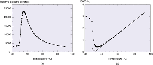
Fig. 6. Temperature dependence of (a) relative dielectric constant εr and (b) 1/εr.
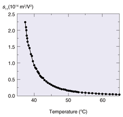
Fig. 7. Temperature dependence of Kerr coefficient s11.
![]()
![]()
![]()
Here, the first term has no relation to the signal. The second term is the same as the refractive index modulation for the Pockels effect. The pseudo Pockels coefficient corresponds to 2s11E0. When we apply a voltage of 100 V between a pair of electrodes whose gap is 1 mm, the Pockels coefficient becomes 2240 pm/V. This is 70 times larger than the value for the effect in LN.
Our beam deflection devices utilize this huge electro-optic effect and the large dielectric constant. Details are explained in another paper in this issue [10]. Here, we discuss the merit in applications to light intensity modulators. The simplest modulator can be fabricated by placing an EO material with electrodes between a pair of crossed polarizers. The half-wave voltage Vπ, which is the voltage difference required to change the transmittance from 0% to 100%, is expressed by
![]()
where λ0, r, d, and l are the wavelength of the light to be modulated, the effective Pockels coefficient, the electrode gap, and the length of the light path in the EO material. Thus, when the effective Pockels coefficient is 70 times larger, we can reduce Vπ to 1/70. If we permit the same Vπ, it is possible to reduce l, that is to shrink the device size. Accordingly, we can expect either a drastic reduction in the load on the voltage controller or significant miniaturization of the modulators.
5. Conclusion
We introduced the growth of KTN single crystals and their electro-optic properties. By carefully controlling the temperature in the TSSG method, we can now reproducibly grow crystals with sizes of more than 30 cm3 with no visible defects. KTN is known for its large Kerr effect. Because of compositional homogeneity, the Kerr coefficient s11 of our crystals exceeded 2.2 × 10⁻¹⁴ m2/V2, which is about 8 times higher than the previously reported value. It also corresponds to a value 70 times larger than the Pockels coefficient for LN when the bias field is 100 V/mm. Great improvements are expected if the EO material in conventional light modulators is replaced with KTN single crystals.
References
| [1] | S. Triebwasser, "Study of Ferroelectric Transitions of Solid-Solution Single Crystals of KNbO3-KTaO3, Phys. Rev., Vol. 114, No. 1, pp. 63–70, 1959. |
|---|---|
| [2] | F. S. Chen, J. E. Geusic, S. K. Kurtz, J. G. Skinner, and S. H. Wemple, "Light Modulation and Beam Deflection with Potassium Tantalate-Niobate Crystals, J. Appl. Phys., Vol. 37, No. 1, pp. 388–398, 1966. |
| [3] | "Successful Preparation of KTN Crystals with the Highest Reported Electro-optic Effect and the Potential for Providing a Great Improvement in Optical Device Performance, NTT Technical Review, Vol. 1, No. 9, pp. 56–58, 2003. |
| [4] | K. Nakamura, J. Miyazu, M. Sasaura, and K. Fujiura, "Wide-angle, low-voltage electro-optic beam deflection based on space-charge-controlled mode of electrical conduction in KTa1−xNbxO3, Appl. Phys. Lett., Vol. 89, No. 13, 131115-1–131115-3, 2006. |
| [5] | "Novel Beam Scanning Phenomenon Using KTN Crystal, NTT Technical Review, Vol. 4, No. 7, p. 54, 2006. |
| [6] | W. A. Bonner, E. F. Dearborn, and L. G. Van Uitert, "Growth of potassium tantalate-niobate single crystals for optical applications, Ceram. Bull., Vol. 44, No. 1, pp. 9–11, 1965. |
| [7] | D. Rytz and H. J. Scheel, "Crystal growth of KTa1−xNbxO3 (0<x<0.04) solid solutions by a slow-cooling method, J. Crystal Growth, Vol. 59, pp. 468–484, 1982. |
| [8] | J. E. Geusic, S. K. Kurtx, L. G. Van Uitert, and S. H. Wemple, "Electro-optic properties of some ABO3 perovskites in the paraelectric phase, Appl. Phys. Lett., Vol. 4, No. 8, pp. 141–143, 1964. |
| [9] | A. Riesman, S. Triebwasser, and F. Holtzberg, "Phase diagram of the system KNbO3-KTaO3 by the methods of differential thermal and resistance analysis, J. Am. Chem. Soc., Vol. 77, pp. 4228–4230, 1955. |
| [10] | K. Nakamura, "Optical Beam Scanner Using Kerr Effect and Space-charge-controlled Electrical Conduction in KTa1−xNbxO3 Crystal, NTT Technical Review, Vol. 5, No. 9, 2007. https://www.ntt-review.jp/archive/ntttechnical.php?contents=ntr200709sp2.html |
 |
|
|---|---|
 |
|
 |
|
 |
|