|
|||||||||||||||
|
|
|||||||||||||||
       |
Special Feature: Applied Technology for Millimeter and Terahertz Electromagnetic Waves Vol. 7, No. 3, pp. 29–34, Mar. 2009. https://doi.org/10.53829/ntr200903sf5 Optical Fiber Electric Field Sensor for Antenna MeasurementAbstractThis article describes an optical fiber electric field sensor that can accurately determine the radiation characteristics of antennas used at frequencies ranging from a few hertz up to the terahertz band. Millimeter and terahertz waves are promising from both the academic and industrial viewpoints and could lead to a broad range of applications in fields such as telecommunications, security, medical therapy, and biology. Characterizing their propagation and radiation will result in improved wireless system designs. 
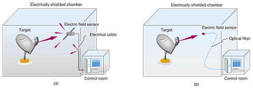
1. Importance of antenna measurementThe millimeter and terahertz radio frequency bands, which were difficult to generate and detect until a few decades ago and thus remained undeveloped, have become intimately linked to technological innovation. The 60- and 76-GHz bands are used for license-free commercial broadband, in-home wireless transmission for high-definition TV and other data, and vehicle radar for automobiles. In NTT Microsystem Integration Laboratories, 76-GHz band signals are used to detect cracks in concrete covered with wallpaper or paint [1]. We are also aiming at practical development of the millimeter and terahertz radio frequency bands by, for example, constructing a 10-Gbit/s fixed wireless access system using the 120-GHz band [2]. Radio frequency resources are both limited by the radio wave laws and inherently scarce, so developing the millimeter and terahertz radio frequency bands in this manner will be an effective way to provide new applications. To make effective use of the radio waves, one must understand their propagation and radiation characteristics in practical usage conditions. Radio wave characterization requires accurate measurement of the antenna, which is the interface between the radio signal and the circuitry. 2. Ideal antenna measurementThe characteristics that are needed to characterize an antenna include the input impedance, directionality, and gain. When any of these characteristics is measured, the accuracy is decreased by external sources of radio waves and the waves scattered by surrounding structures. The ideal situation, then, is to perform the measurements in free space where no external radio waves affect the antenna measurement or in an electromagnetically shielded room. At the same time, the electric field sensor used for detecting the signal from the antenna should not affect the signal being detected. Currently, a standard dipole antenna, such as shown in Fig. 1(a), or a horn antenna is used as the electric field sensor, and the detected signal is carried by an electrical cable to the measuring instrument. The sensor and cable are made of metal, which scatters the signal emitted by the antenna being measured. That may make it impossible to know the original state of the signal. In particular, if the sensor is placed near the antenna under test, electrical coupling occurs and radio waves other than the free-space propagating signal arise. An ideal measurement setup requires the use of a metal-free electric field sensor and a non-metallic cable, such as an optical fiber, as shown in Fig. 1(b), for accurate measurement of the radio signal.
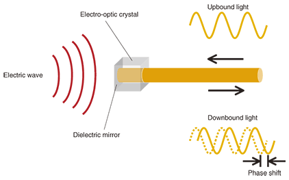
3. Optical fiber electric field sensorWe utilized the electro-optic (EO) effect to develop an electric field sensor that contains no metal. The EO effect is a phenomenon in which the natural refractive index of a material changes when an electric field is applied. When the change in refractive index is directly proportional to the electric field strength, it is referred to as the Pockels effect [3]. The sensor that we developed uses an EO crystal that exhibits the Pockels effect. Using the Pockels effect in measuring an electric field requires some means of measuring the change in refractive index caused by the applied electric field. We use the phase change of light passing through the EO crystal being irradiated by radio waves (Fig. 2). In the absence of electromagnetic radiation, there is no change in refractive index, so there is no change in the phase of the light passing through. In the presence of radio waves, the refractive index varies in proportion to the electric field strength, so the phase of the light passing through changes. The magnitude of that phase change can be used to calculate the strength of the electric field acting on the crystal. In Fig. 2, light that has propagated in free space is input to the EO crystal; however, because it is difficult to control light propagating over a long distance in free space, the configuration shown in Fig. 1(b) is impractical. For light propagating over a long distance, it is appropriate to use optical fiber, which was developed in the field of telecommunications. Nevertheless, changes in the optical phase of light propagating through the optical fiber caused by bending and by temperature changes randomize the phase of the light reaching the EO crystal, creating dispersion in the sensor’s measurement sensitivity. To prevent that effect, we fixed the optical fiber of our sensor in a glass tube so there was no phase change, even when the sensor was moved. Nevertheless, the glass tube holding the optical fiber inside is several tens of centimeters long, so the propagation of light from the sensor tip in the electromagnetic shield room to the control room is problematic (Fig. 1).
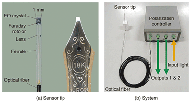
We therefore developed a technique for achieving zero phase change in the optical fiber by using the fact that the same phase change is applied to both the upbound and downbound lights at the midpoint of the EO crystal to cancel out those phase changes. In this way, we succeeded in making the optical fiber that connects the sensor tip to the control system easy to handle. The configuration of the developed optical fiber electric field sensor is shown in Fig. 3. The size of the EO crystal is 1 mm3, the same size as a conventional optical fiber electric field sensor. The sensor’s tip comprises an EO crystal with a dielectric reflector, a Faraday rotator, lens, ferrule, and optical fiber. The sensor is connected to a polarization controller that adjusts the polarization by using a 5-m length of optical fiber, as shown in Fig. 3(b). The sensor is connected via the polarization controller to a light source and photodetector. We confirmed that, theoretically, the system will operate with stable sensitivity even if the optical fiber is extended to a length of 1 km.
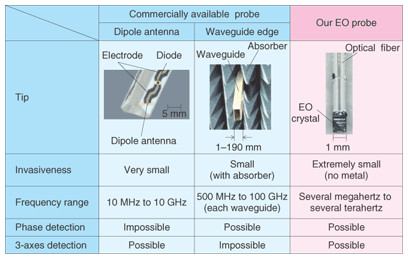
4. Sensor’s featuresAn electric field is disturbed only very slightly by the optical fiber electric field sensor, so this sensor is particularly effective for measurements close to the measured object. When the radiation characteristics, known as the antenna pattern, are measured, it is usually necessary to arrange the sensor at a sufficient distance from the test object in order to measure the electric field distribution over a very wide range. If we consider, for example, the 2-GHz band, which is used for cell phones, the sensor must be scanned over distances of several meters inside a cubical shielded room that is several meters on a side. In recent years, a method for calculating the antenna pattern from an electric field distribution measured closer to the object being measured has been developed to reduce the size of the measurement environment. In addition to solving the problem of a large measurement environment, this method can greatly shorten the measurement time. To make accurate near-field measurements, it is important to prevent the electric field from being disturbed (Table 1). Furthermore, antenna pattern calculation requires measurement of the electric field strength and phase along three orthogonal spatial axes. Our sensor satisfies these requirements and is the only technology currently applicable to the frequency range from a few hertz to several terahertz.
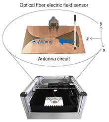
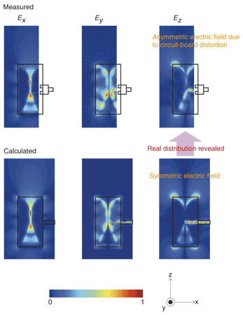
5. Antenna near-field measurement systemAn antenna near-field measurement system using the optical fiber electric field sensor is shown in Fig. 4. The sensor is mounted on an XY stage and scanned in two dimensions over the antenna being measured. The antenna is surrounded by radio wave absorbers to decrease unwanted reflections from the walls. The entire system is electrically shielded to exclude external electromagnetic interference. The electric field distribution in a plane 0.5 mm above the antenna base is shown in Fig. 5. An 8-GHz sine wave signal was input to the antenna and the sensor was scanned in two dimensions, 150 mm along the z axis and 50 mm along the x axis. The upper part of Fig. 5 shows measurement data from the sensor; the lower part shows the calculated results of a numerical simulation. The x- and y-axis measurement results agree well with the computed values, indicating that the measurement accuracy was high. The z-axis measurement results differed from the computed results, revealing a bias in the electric field distribution. That was caused by a slight nonuniformity in the distance between the sensor and antenna during measurement resulting from distortion in the antenna. The bias also appeared in the data for the x and y axes, but the sensitivity to distance was greater for the z axis, so the bias in the electric field distribution could be measured. That shows that while a numerical simulation can produce only the ideal electric field distribution, the measurement results can reveal minute errors in manufacturing processes and other things that may point to problems in the actual antenna design. Although not presented here, we also confirmed the consistency of three-axis electric field distribution measurements of the phase and of the numerical analysis. We also confirmed that measurement of electric field distributions at frequencies up to 60 GHz was possible. While our optical fiber electric field sensor can be used up to the terahertz band, the upper frequency limit for measurement is determined by the light source for input to the sensor. We are currently investigating the optimum light source for evaluating the 120-GHz band antenna being developed within our group.
6. Concluding remarksWe transferred this technology to the Research Laboratories of NTT DOCOMO Inc. in 2005 and collaborated with them to measure the relative absorption rates of cell phones. We also presented a working exhibit at Wireless Technology Park 2008 held at Pacifico Yokohama in May 2008, which was highly acclaimed by many people as demonstrating a technique capable of ideal antenna measurement. Our goals for future work include a near-field/far-field conversion algorithm for the optical fiber electric field sensor and an antenna measurement system useful for antenna design. References
|
||||||||||||||