|
|||||||||||||||||||||||
|
|
|||||||||||||||||||||||
|
Regular Articles Vol. 13, No. 5, pp. 33–38, May 2015. https://doi.org/10.53829/ntr201505ra1 InP-based Membrane Optical Devices for Large-scale Photonic Integrated CircuitsAbstractLarge-scale photonic integrated circuits for telecom and datacom applications have attracted attention for many years. We have developed III-V based membrane optical devices employing lateral p-i-n junctions with buried heterostructures. This article introduces lateral current injection lasers and modulators integrated on an InP substrate and membrane lasers on a SiO2/Si substrate as promising building blocks of integrated transmitters. Keywords: semiconductor laser, modulator, photonic integrated circuit  1. IntroductionNetwork traffic is increasing exponentially along with the explosive growth of social media [1]. The development of optical fiber networks has made it possible to achieve high-speed, large capacity, and reliable networks. Device integration has been a key technology in reducing power consumption in electronic and optical devices, making it possible to achieve environmentally friendly networks. Large-scale electronic integration based on complementary metal-oxide semiconductor (CMOS) technology has contributed to the development of high-performance processers and memories with low power consumption. We have now entered an era of photonic integration. Integrated photonic devices such as transmitters and receivers are now available thanks to the advances in fabrication technology. Photonic integrated circuits (PICs) have been developed to provide the following benefits: (1) compactness, (2) a reduction in the number of components, (3) low power consumption, (4) low-cost fabrication, and (5) integration of photonics and electronics. Semiconductor platforms consisting of III-V semiconductors* and silicon have been developed to meet these requirements. Wavelength-division multiplexing (WDM) is employed in telecom networks to transmit optical signals. This involves the use of integrated optical devices such as an electro-absorption (EA) modulator integrated distributed feedback (DFB) laser and a tunable DFB laser array on an InP substrate. However, the numbers of devices and functions have been limited. Recently, advanced modulation formats, which use a combination of amplitude and phase modulation, are triggering higher density integration for core and metro networks. InP-based large-scale monolithically integrated transmitters and receivers consisting of more than 100 optical components have been reported [2]. Because the number of components is increasing, these photonic integration technologies are promising in their potential to reduce assembly costs and footprints. In addition, photonic networks have been expanded to short reach applications such as in access networks and datacom networks. Laser arrays and detector arrays are now used in 100-Gigabit Ethernet transceivers [3]. Each discrete device operates at the speed of 10–25 Gbit/s. The trend in using photonic integration is obviously growing because of the need to reduce the cost and power consumption of networks. In datacom applications, multi-mode VCSELs (vertical cavity surface emitting lasers) are used as light sources for inter- or intra-board transmissions. In the future, WDM transmitters based on integrated single-mode laser and detector arrays will be essential to increase the transmission capacity. Silicon photonics have been actively demonstrated for a wide range of applications [4, 5] and show promise in meeting the above requirements. Although the integration of light sources is a challenge, most of the functions of PICs have been implemented on silicon. Therefore, further integration of III-V and silicon photonics devices are expected to complement each function. Two other factors are important in order to make further progress: device structure and fabrication. Most optical devices consist of laser/amplifier, modulator/photodetector, and passive waveguide regions; we can fabricate every optical device for every target application by combining these components. Our aim is to develop a flexible and scalable fabrication technique implementing this concept. In this article, we introduce membrane devices consisting of lateral p-i-n junctions as building blocks for PICs. We employ a selective doping technique to fabricate the p-i-n junctions, as it enables flexible device fabrication. We first clarify the advantages of membrane optical devices. Then we describe lateral current injection lasers and modulators fabricated on InP substrates for telecom applications. Finally, we discuss III-V optical devices on silicon substrates employing novel fabrication techniques. We also introduce lateral current injection lasers on SiO2/Si substrates for datacom applications.
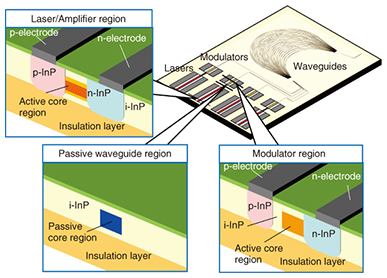
2. Concept of photonic integrationOur concept of photonic integration consists of InP-based membrane optical devices (Fig. 1). The figure illustrates an example of an integrated transmitter consisting of lasers, modulators, and waveguide regions. Each active region employs a lateral p-i-n structure along the substrate. The electrodes are fabricated on the surface to apply electrical voltage along the lateral direction. We use selective doping techniques to fabricate the p-i-n regions. Each impurity doping region is fabricated on a non-doped epitaxial layer that includes the active and waveguide regions. The selective doping technique is common in CMOS fabrication processes, as it enables mass production.
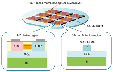
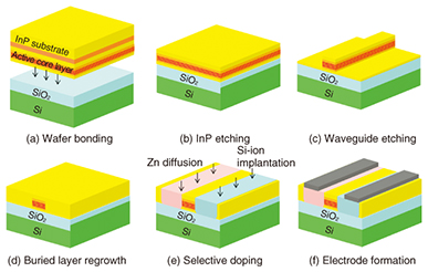
This configuration provides higher scalability and productivity compared with conventional devices employing vertical p-i-n structures. Generally, the optimum doping condition is different for each active component. In particular, non-doped regions are essential as the passive waveguide regions in order to suppress the optical propagation loss. Conventional devices with vertical p-i-n junctions require a number of crystal regrowth processes to integrate optimized components. Our approach can form impurity-doped regions without using epitaxial regrowth processes; in other words, the number of regrowths decreases. In addition, assembly with electrical components is easy because the electrodes are formed on one side. These applications are not limited to PICs on an InP substrate. We propose a novel process to fabricate III-V devices on silicon. Our approach is shown in Fig. 2. This process uses a template consisting of III-V layers bonded on a silicon substrate. The butt-joint sections, waveguides, buried heterostructures, and doping regions are formed on this template. The use of large silicon wafers improves the yield. In addition, the alignment of III-V devices on the silicon substrate is possible with a level of accuracy in the sub-micrometer range. Therefore, III-V active devices can be easily integrated with silicon photonic devices including silicon-based waveguide structures. Typical fabrication procedures are shown in Fig. 3: (a) a III-V wafer including active layers is bonded on a SiO2/Si substrate; (b) the InP region is removed; (c) waveguides are fabricated by etching; (d) buried heterostructures are fabricated by epitaxial regrowth; (e) p- and n-doped regions are formed by Si-ion implantation and Zn thermal diffusion; and (f) electrodes and surface gratings are formed.
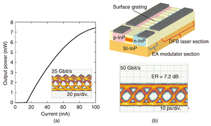
The membrane devices have some advantages in both their device characteristics and their fabrication [6]. A lateral buried heterostructure with a p-i-n junction has lower capacitance compared with vertical p-i-n structures. This feature provides high-speed operation of lasers, modulators, and photodetectors due to the small RC (resistor-capacitor) time constant. In addition, introduction of III-V slab layers sandwiched by low refractive index materials improves the power consumption because of the strong optical confinement. This is advantageous in reducing the power consumption of PICs for short-reach datacom applications. In the next section, we describe the fabrication of lasers and modulators on InP and lasers on silicon. 3. Membrane devices on InP substrate: lasers and modulatorsWe fabricated lateral current injection DFB lasers [7] and EA modulators on an InP substrate [8]. The DFB lasers were fabricated using processes similar to those in Fig. 3 except for the wafer-bonding related processes in Fig. 3(a) and (b). The DFB laser consists of an InGaAlAs-based 14-well active region. A λ/4-shift grating is formed on the InP surface. The static and dynamic characteristics of a laser with a length of 400 μm are shown in Fig. 4(a). The single-mode lasing was observed at room temperature. The threshold current was 14 mA. This laser achieved 25-Gbit/s direct modulation as shown in the inset. This was the first demonstration of direct modulation over 25 Gbit/s for a lateral current injection laser. We also developed an EA-DFB laser employing lateral p-i-n junctions. The device structure and modulation waveform are shown in Fig. 4(b). The modulator section consists of an 8-well InGaAlAs active region. The EA length is 200 μm. This structure does not exhibit a quantum-confined stark effect, which is an operating principle of conventional quantum-well EA modulators with vertical p-i-n structures. However, we theoretically confirmed a practical optical extinction ratio without sacrificing the modulation speed. The fabricated EA-DFB laser operates at a static extinction ratio over 20 dB. In addition, 50-Gbit/s modulation with a dynamic extinction ratio of 7.2 dB is obtained. This is the first demonstration of a lateral EA-DFB laser. As a result, a sufficient modulation speed for 100- and over 100-Gbit/s laser arrays for telecom applications has been demonstrated.
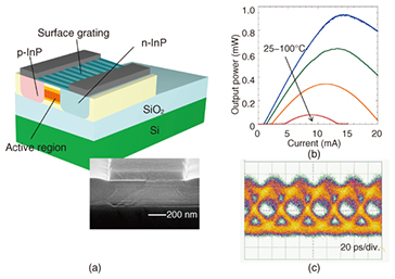
4. Directly modulated lateral current injection lasers on SiO2/SiWe also developed membrane DFB lasers on SiO2/Si [9, 10]. A schematic of the device structure and an SEM (scanning electron microscopy) image of the cross section are shown in Fig. 5(a). The device consists of a 6-well InGaAsP-active region. The laser was fabricated according to the processes shown in Fig. 3. Suppressing degradation of the III-V epitaxial layer during the fabrication process is a challenging task. Thermal stress is induced during the fabrication because the thermal expansion coefficients are different between the InP, SiO2, and Si layers. This stress can cause cracks in the III-V layer. Introduction of a III-V layer that is thinner than the critical thickness under the induced strain solved this problem. Consequently, we successfully fabricated the buried heterostructure without serious degradation by employing the 250-nm-thick III-V layer that included the active region. The current-light output characteristics of the DFB laser are shown in Fig. 5(b). The cavity length is 73 μm, and the threshold current is 0.9 mA at a temperature of 25°C. Regardless of the high thermal resistance due to the SiO2 layer, lasing operation was observed up to 100°C. The laser achieved 25.8-Gbit/s direct modulation as shown in Fig. 5(c). The bias current was 3.2 mA. The energy cost of the data transmission was 171 fJ/bit, which is the smallest value of all DFB lasers. We also achieved 40-Gbit/s direct modulation by employing another structure. These results show the feasibility of low-power consumption operation of membrane lasers on SiO2/Si.
5. SummaryWe have presented InP-based membrane optical devices for large-scale PICs for network applications. These devices achieve practical performance as well as simple and scalable fabrication processes by means of selective doping techniques. We successfully demonstrated DFB lasers and EA-DFB lasers fabricated on InP, and DFB lasers fabricated on SiO2/Si. All of these devices achieved modulation characteristics applicable to 100-Gbit/s or higher transmitters. In particular, the directly modulated lasers on SiO2/Si have the smallest energy cost of all DFB lasers: 171 fJ/bit. We believe these achievements pave the way for further development of large-scale PICs on various platforms including InP and silicon for a wide range of network applications. References
|
|||||||||||||||||||||||