|
|||||||||||
|
|
|||||||||||
       |
Feature Articles: Photonics-electronics Convergence Technology to Achieve All-Photonics Network Vol. 18, No. 10, pp. 12–15, Oct. 2020. https://doi.org/10.53829/ntr202010fa1 All-Photonics Network and Photonics-electronics Convergence Technologies as a Vision of the FutureAbstractThis article presents the Innovative Optical and Wireless Network (IOWN) proposed by NTT and the All-Photonics Network—a key element of IOWN—as a vision of the future along with the technologies for achieving it. It also introduces photonics-electronics convergence technologies as the key to achieving an ultralow-latency and ultralow-power consumption of the All-Photonics Network and its roadmap. Keywords: IOWN, All-Photonics Network, photonics-electronics convergence
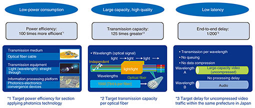
1. What is IOWN?NTT aims to build a prosperous society in which people recognize diverse concepts of values. Obtaining information and sensations from another person to deepen mutual understanding should contribute greatly to achieving such a new and highly diverse world. To achieve this world through research and development, there will be a need not just to obtain large amounts of information through communication infrastructures that are more massive than ever before but also to process that information on a level that includes human feelings and subjectivity. Toward achieving this future vision, NTT has put forward the concept of the Innovative Optical and Wireless Network (IOWN) as an unprecedented communications platform. The aim is to achieve a network and information-processing platform featuring ultralarge-capacity, ultralow-latency, and ultralow-power consumption capabilities through innovative technologies centered around photonics. NTT has started to discuss with various partners toward achieving IOWN in 2030. IOWN consists of three key elements: the All-Photonics Network (APN), which introduces photonics-based technologies throughout the network even as far as user’s terminals in an end-to-end manner; Cognitive Foundation®, which centralizes management, operation, deployment, configuration, and interlinking of information and communication technology resources in different devices such as edge computers, network services, and user equipment, all from the cloud; and Digital Twin Computing as a new computing paradigm that combines many items of digital information representing the real world and simulates different forms of interaction between objects and humans in cyberspace. Each of these elements targets a different layer, but in combination, they can achieve a new generation of networks and information processing. 2. Importance of the APNAmong the above three elements, the APN is the foundation of new optical communications and information processing. As its most outstanding feature, it is aimed at achieving an information-processing infrastructure with low-power consumption and high-speed information transmission through a transition from conventional electronics to photonics (Fig. 1). The target power consumption is to increase power efficiency by 100 times through the introduction of the photonics-electronics convergence technologies described below. The target transmission capacity, meanwhile, is a 125-fold increase made possible by, for example, the development of multicore fiber that accommodates many cores within a single optical fiber and the development of a coherent optical subassembly. Furthermore, the target end-to-end delay is 1/200 of the current level by, for instance, transmitting data in uncompressed form in the case of applications that cannot allow for any delay.
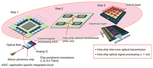
3. Examples of diversity and application through the APNWhen the APN is achieved, we can expect various new scenarios. Due to the limited bandwidth of a current network, the amount of data in information to be transmitted has been purposely reduced using a technique such as sampling, quantization, and data compression when analog data are converted to digital data. In contrast, the dramatic leap in transmission capacity in the APN will make it possible to send and receive information with high resolution and a high sampling rate, which is faithfully closer to the original signal. Furthermore, if data that cannot be perceived by humans, such as a bee’s sense of sight, dog’s sense of smell, or bat’s sense of hearing, are maintained and exchanged without data compression, it should be possible to greatly extend the five human senses and create a society that enhances the human capability of empathizing with others. If different optical wavelengths were to be allocated to each different function and service in optical fiber transmission, it would be possible to transmit multiple streams of information simultaneously with low latency. For example, interactive exchanges between people with no delay could take place while transmitting high-definition images over multiple channels. As a result, applications with critical requirements for communications quality, such as remote surgery and mobility as a service, could be made practical. 4. What are photonics-electronics convergence technologies?To successfully achieve the APN, we should introduce photonics-electronics convergence technologies, which combine electronics and photonics technologies in the signal processing section of a processor chip. This extends the role of photonics, which has conventionally been used for long-distance and medium-distance transmission such as in interconnects within datacenters. NTT laboratories achieved a milestone in the development of photonics-electronics convergence technologies by fabricating an optoelectronic conversion device that operates on the world’s smallest amount of consumed energy. This achievement was published in the British scientific journal Nature Photonics on April 15, 2019 [1]. Technology for integrating light with part of an electronic circuit has been investigated for over 20 years, but large device size and power consumption prevented this technology from becoming practical. The technology presented by Nozaki et al. [1] succeeded in cutting power consumption by 94% compared with current technology. The roadmap for photonics-electronics convergence technologies is shown in Fig. 2. The first step will be to fabricate a structure that integrates circuits using silicon photonics with fibers and analog integrated circuits (ICs) and achieve ultrahigh-speed connections with peripheral circuits outside the chip (Step 1). The next step will be to directly interconnect chips by ultrashort optical wiring to improve information processing performance (Step 2). The last step will be to lower power consumption by interconnecting cores within a chip by optical wiring and applying optical transistors. We also aim to achieve arithmetic processing instantly only in the light propagation time of the optical circuit by using optical pass gate technology, which make maximum use of optical characteristics (Step 3).
5. Content of feature articlesThe Feature Articles in this issue take up photonics-electronics convergence technologies toward the APN at the NTT Science and Core Technology Laboratory Group. They will introduce the above steps: Step 1 achieving ultrasmall optical transmit/receive circuits using silicon photonics technology [2], Step 2 targeting high-density, low-power optical interconnections [3], and Step 3 focusing on optoelectronic conversion devices and optical pass gate circuits using nanophotonics technology [4]. References
|
||||||||||