|
|||||||||||||||||||||||
|
|
|||||||||||||||||||||||
       |
Feature Articles: Optical Device Technologies for Next-generation Computing Using Light Vol. 20, No. 8, pp. 58–63, Aug. 2022. https://doi.org/10.53829/ntr202208fa8 Photonic Implementation of Reservoir ComputingAbstractToday’s computing for machine learning is carried out with digital electric processors, which have issues regarding energy consumption and processing speed, by emulating brain-inspired information processing. To address these issues, photonic devices, comprising a photonic neural network, are gaining much attention for achieving high-speed and energy efficient brain-inspired computations. We report on the photonic implementation of a simplified recurrent neural network called reservoir computing. Keywords: photonic computing, machine learning, reservoir computing
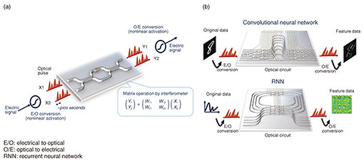
1. IntroductionRecent large-scale information-transportation technology has been driven by the development of photonic devices, such as photonic transceivers, receivers, and switches. Due to these technological developments, the barrier between photonics and electronics has been lowered, which enables the integration of photonic and electric circuits into a single module. Such optoelectronic integration technology is now advancing for much larger-scale and energy-efficient optical transmission [1]. Optoelectronic integration has been gaining attention for applying photonic circuits as computation units, such as logic gate [2], matrix operation [3] and/or optimization solver [4], beyond the simple optical link function. These studies revived the development of optical computing, which was intensively studied during the 1980s. This revival is also related to the explosive evolution in artificial intelligence (AI). Information processing in AI involves brain-inspired computational algorithms called artificial neural networks (ANNs). Their computation is based on a huge amount of matrix operations and nonlinear processing, which requires energy-hungry large-scale computational resources. As the demand for such computation is explosively increasing, the development of special-purpose AI hardware providing much faster and more energy-efficient computational resources has been intensively studied. The photonic implementations of ANNs are attracting interest because they have potential to reduce operational power, increase speed, and reduce latency beyond what is possible in electronic computing. Unlike digital calculation on conventional electronic circuits, photonic computing uses analog values, such as the intensity and phase of optical signals, as information. Its propagation and interference are considered as the computation. For example, when we input an optical signal to an optical interferometer, as shown in Fig. 1(a), the optical signals interfere with each other. The output intensities can be considered the results of the matrix product of the input signals and parameters in the interferometer. This calculation is conducted only by high-speed light propagation and interference without principle energy consumption. More large-scale computation is possible by using the optical signal multiplexing technologies developed for telecom application, such as time, wavelength, and space division multiplexing. We can construct various ANNs by designing the configuration of an optical interference system, as shown in Fig. 1(b).
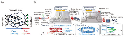
2. Reservoir computing and its photonic implementationReservoir computing (RC) is a type of recurrent neural network having recursive connections, as shown in Fig. 2(a). In the RC framework, the weights of the input and reservoir layers are randomly fixed and not trained. Only the output weights are trained by linear regression such as the least squares method, which is much simpler than the training method used in standard ANNs such as backpropagation. In spite of the simple configuration, RC has shown excellent performance comparable to that of standard ANNs on a series of benchmark tasks such as speech recognition, economic forecasting, and action detection in video data. RC also has advantages from the viewpoint of photonic implementation. Standard deep ANNs require fine tuning of each weight through the use of the error back propagation algorithm, which requires highly accurate and uniform large-scale integration of tunable optical elements, which is a challenging issue for fabrication. The training time of a photonic ANN is generally much longer than that with electrical devices because the reconfiguration of optical weights takes milliseconds. In the RC framework, however, there is no need for any fine tuning of the optical system under training. As the training time is determined by forward propagation in RC, it can be accelerated using photonics. Thus, we focused on this configuration at the first stage of photonic implementation of an ANN. Figure 2(b) shows our previously proposed device architecture for photonic RC [5]. In the input optical circuit (left side in figure), the optical signal is weighted along the time and space directions, which emulate the input layer of RC. In the circuit for the reservoir layer (right side in figure), a ring-shaped optical cavity array represents a recursive coupling of neurons, emulating the reservoir layer of RC. The output signals from the reservoir optics are converted to an electric signal by using a photodetector (PD). By weighting the output signals on the electric digital circuit, we can obtain a final output signal of RC. We implemented our RC architecture using a silica-based optical waveguide technology called planar lightwave circuit (PLC), which was originally developed for optical telecom devices. Our PLC acts as photonic RC with 512 reservoir neurons, which is over 30 times larger than in previous on-chip photonic implementations. The PLC can execute the multiply and accumulate operations beyond 20 tera times per second for each wavelength and reach peta-scale computation speed on a single photonic chip by using wavelength division multiplexing. This value is beyond recent electronic computation. We experimentally confirmed the performance of our PLC using standard benchmark tasks such as hand-written-digit classification. We could classify hand-written-digits images with an accuracy of 91.7% and ultrafast processing speed of 17.1 ns per image. This accuracy and speed is the highest for on-chip photonic RC implementation.
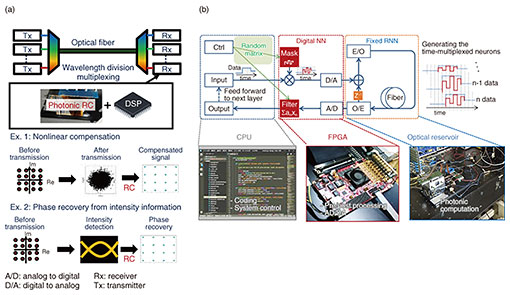
3. Application of photonic RCAs one of the features of photonic computation is its high-speed processing, we believe that it is suitable for applications that can use this advantage. An example of such an application is signal processing for optical communication, as shown in Fig. 3(a). In recent optical communication, the distortions of the transmitted optical signals are compensated for using a digital signal processor (DSP). Its computational costs, however, becomes an issue to increase the communication capacity. When we use the photonic ANN including RC as the signal processor for such application, we can outsource the computational costs of a DSP to the photonic processor [6]. We are also studying a method for drastically simplifying the coherent receiver configuration by using photonic RC [7]. We are also considering the application of photonic RC to more general machine learning tasks. For such application, it is important to develop the hardware/software interface between photonic RC and a standard computation device such as a central processing unit (CPU). Therefore, we built a test platform of photonic RC using a field-programmable gate array (FPGA)-based hardware interface and Python-based software stack (Fig. 3(b)). The user can drive the optical RC system like standard computation hardware using a standard programming language (Python/Pytorch). We have also experimentally confirmed its superior performance [8].
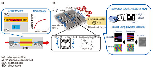
4. Toward improving performance of photonic RCTo further improve the processing performance of photonic RC, it is essential to improve and harness the functionalities of photonic devices. For example, nonlinear optical effects should be more positively exploited for optical implementation of neurons, while in conventional optical communication they have been intentionally suppressed due to undesirable signal distortion. However, it is difficult for silica-based PLCs to implement such nonlinear functionalities; thus, in the above-explained physical implementation, the nonlinear functionality was implemented opto-electronically, necessitating optoelectronic conversion. Photonic devices based on III-V semiconductors, such as an optical amplifier, can be used as all-optical nonlinear elements. By heterogeneously integrating such III-V devices on silicon photonics, nonlinear activation can be implemented all-optically even on photonic integrated circuits (PICs). To this end, we used our recently developed III-V semiconductor optical amplifier (SOA) on silicon shown in Fig. 4(a) to implement an all-optical nonlinear reservoir. We then experimentally evaluated its processing performance via a nonlinear benchmark task, and it was shown that the obtained performance was as good as those of typical RC with optoelectronic nonlinearity [9]. On the basis of this achievement, we are considering integrating such nonlinear functionalities on PICs toward further performance improvement of photonic RC. In addition to the optical nonlinear implementation, large-scale optical integration of neurons is essential. Although the state-of-the-art ANN requires about 10 billion weight parameters, it is currently difficult to implement such a large-scale model with an optical ANN or RC system. The scalability of a photonic ANN is basically limited by the size of optical gate element shown in Fig. 1(a). As its typical size is about 100 μm square, it is difficult to implement the large-scale state-of-the-art ANN into standard optical circuits with a realistic footprint. We previously proposed a framework that uses lightwave propagation as a neural network, as shown in Fig. 4(b) [10]. In this framework, we can consider the distribution of the refractive index in the optical circuit as the weight of the neural network. Since the refractive-index distribution can be controlled to 1-μm2 pixel size, we can achieve large-scale implementation of an optical ANN and RC about 1 million times that of the conventional method. We confirmed that the performance of the proposed wave-equation-based neural network is comparable to one for the state-of-the-art ANN. By using such new processing methods, we are now developing a photonic computation platform toward future ultrafast information processing.
5. SummaryWe gave an overview of recent developments in our photonic implementation of a special type of neural network called RC. By using the nature of light, photonic RC can achieve high-speed, low-power parallel computing beyond the conventional electronic processor. We also introduced its potential application and performance improvement. In spite of the attractive features of photonic computation, the re-invention of the computer using photonic technology is still not easy. We will continue to further conduct research on a future photonic computing platform by considering the entire computing system and algorithms beyond device-level approaches. References
|
||||||||||||||||||||||