|
|||||||||||||||||||||||||||
|
|
|||||||||||||||||||||||||||
|
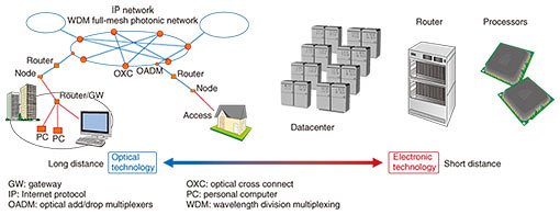
Feature Articles: Forefront of Research on Integrated Nanophotonics Vol. 16, No. 7, pp. 1–7, July 2018. https://doi.org/10.53829/ntr201807fa1 Nanophotonic Technologies for On-chip Photonic IntegrationAbstractOur research group has been conducting basic research that seeks to introduce optical networking technology in processor chips. Using nanophotonic technology as represented by photonic crystals as the base, we are researching nanophotonic integration technologies to microminiaturize optical devices, drastically reduce energy consumption, and create a variety of new functions. In the Feature Articles in this issue, we introduce our latest achievements in creating nanophotonic devices and our efforts in developing new optical computing technologies using nanophotonics as the base. Keywords: integrated nanophotonics, photonic crystal, photonic integrated circuit  1. IntroductionInformation technology has become a critical technology for supporting our infrastructure for daily life. The history of information technology is marked by optical signals replacing electrical signals for long-distance communication, and this change is gradually extending to short-distance communication (Fig. 1). This trend is taking place due to bandwidth limitation in copper wires, as high bit-rate communication is not possible, and large-capacity signals cannot be sent when transmitting long-distance electrical signals over the wires. Currently, fiber-to-the-home has already become widespread, and the communication system components have become optical-based. In view of this trend, our research group is carrying out research to incorporate optical network technology in processor chips.
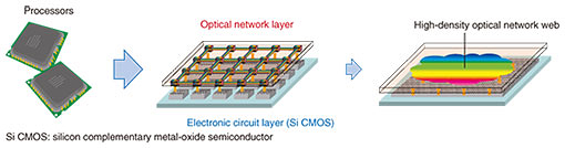
Electrical signal processing has been thought to be optimal for short-distance systems such as a processor chip. However, we believe that optical information processing technologies are necessary in future chips for two reasons that we explain below. The reasons are slightly different from the reasons optical fibers replaced copper wires. Current processor chips face the problem of dramatically increasing power consumption as performance grows. Miniaturized wires and the network between cores consume a large portion of energy in a chip. This heavy consumption occurs due to Joule heating by electrical resistance of wires. In addition, the speed is limited by RC delay (resistance and capacitance of electrical lines). As a result, when the bit rate is high, energy consumption increases. Optical information transfer is not limited by RC delay nor Joule heating, so light does not need more energy than electrical lines at a high bit rate. This is the first reason we seek to deploy optical technology in chips. In the future, it will be necessary to reduce the amount of energy consumed per bit in order to improve processor performance. Electrical information transfer is believed to have a lower limit of several tens of femtojoules per bit due to RC limitations. This is not a serious problem at present, but in 10 to 15 years there will be a need to overcome this barrier. Optical technology is considered a possible means for hurdling past this wall. As shown in Fig. 2, we envision that optical technology will be incorporated in future chips and will work in concert with complementary metal-oxide semiconductor (CMOS) electronic circuits [1].
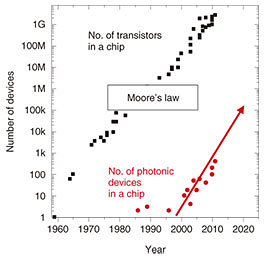
The other reason for incorporating optical technology into chips is related to a processor’s computational latency. Although processor performance is improving at present as described by Moore’s law, the bandwidth of transistors itself is already saturated, leading to high latency; performance improvements are mainly a result of technological developments such as parallelization. However, when true low-latency processing is required, the latency of existing processor chips becomes a problem. In the future, our society will become a cyber-physical system society in which the real world (physical world) and the cyber world will be intimately connected. In such a society, vast amounts of information from the real world serve as input that requires an immediate response from the cyber world, and computational latency will become a critical problem. As discussed below, optical technology has the possibility of dramatically reducing computational latency. This is another reason we seek to develop optical technologies that can be deployed in chips. Next, we consider what kinds of technologies are necessary to address the issue of high computational latency. 2. Necessity of integrated nanophotonicsTo introduce optical networking technology and optical computational technology in processor chips, it is necessary to integrate a great number of ultrasmall optical devices on a processor chip. However, since it is inherently difficult to confine light in a small space, in general, optical devices are overwhelmingly larger than electronic devices, presenting difficulties for integration. We show in Fig. 3 the degree of integration of electronic devices over the years for which Moore’s law has been famous, and for comparison, the integration of optical devices. The scale of optical device integration began to take off in around 2000 and has been rising at about the same rate as Moore’s law. However, this trend will approach a limit in the near future due to the current size of optical devices. Unless optical devices become dramatically smaller, future improvement in the scale of integration cannot be expected.
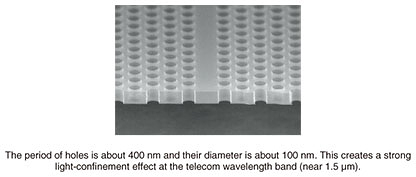
We are seeking to develop technologies that can integrate about 1 million optical devices on a chip. However, this goal is difficult to achieve with existing technologies. In addition, simply reducing the size of devices is not sufficient. It is also necessary to reduce the energy consumption of each device. Current optical devices consume about 1 to 100 pJ per bit. As noted above, the information transmission cost of light is low. However, no matter how low the transmission cost, it means nothing for the achievement of our goal if optical devices consume energy in the picojoule range. Therefore, there is a need to reduce their energy consumption to 1/1000th of the current level. As described above, unless there are major breakthroughs in the degree of integration and energy consumption in the future, it will be difficult to integrate a great number of optical devices on a chip. To achieve this goal, we believe that the nanophotonic integrated technologies described in the next section are necessary. We are therefore conducting research on integrated photonics. Nanophotonics comprises various technologies. We introduce one of them here, the photonic crystal* [2, 3]. A photonic crystal is an artificial structure that modulates the refractive index with a periodicity of about 100 nm. It is known for its ability to realize a variety of new physical properties that cannot be achieved with conventional materials. Especially notable of these features are strong light confinement and light-matter interaction enhancement. As a result, photonic crystals are effective for miniaturizing optical devices and reducing energy consumption. An example of a silicon-based photonic crystal is shown in Fig. 4. The creation of this structure was made possible by applying NTT laboratories’ cutting-edge semiconductor processing technologies.
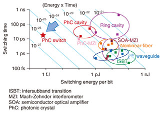
3. Developments in microminiaturization and low-energy consumptionOur research group has developed a variety of optical devices using photonic crystals. The size of all of the devices is about several micrometers, which is 1/100th to 1/1000th the size of conventional optical devices. Energy consumption thus can be dramatically reduced. The graph in Fig. 5 compares the energy consumption of various optical switches and their switching energy. For conventional devices, the products of the energy consumed and the switching time lie nearly on a straight line, indicating a trade-off. However, photonic crystal switches [4] are found in an area where the product of energy consumption and switching time is three orders of magnitude smaller. In fact, this product is mostly determined by the device’s size. Because a photonic crystal’s strong light confinement makes it possible to reduce the device size, ultralow-energy consumption can be achieved without losing switching time.
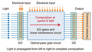
This principle can also be effectively applied to other types of devices, and we have achieved substantial improvements in low-energy consumption for optical memory devices [5] and laser devices [6]. We have also succeeded in integrating more than 100 bits of optical memory to work together as multi-bit memory, demonstrating the first integration of more than 100 devices in nanophotonics [7]. With our recent research, we seek to further reduce device size. One promising technology for this is plasmonics technology, which is introduced in the article “Toward Application of Plasmonic Waveguides to Optical Devices” [8] in this issue. The technology creates nanoscale structures with metals such as gold, and plasmon modes produced on the metallic surfaces are used to confine light. Use of plasmonics results in some amount of additional loss of light, but light can be confined to a smaller area than with photonic crystals. It has been difficult to couple light from the outside for plasmonic structures. However, we have developed and tested a structure that couples a plasmonic waveguide that confines light to a region that is 1/1000th of the wavelength with a conventional silicon waveguide. Going forward, we seek to further miniaturize devices by using this structure, and we seek to make advances in the high-performance region shown in Fig. 5. 4. Impact of ultralow capacitanceWe have explained that nanophotonic technology enables the miniaturization of devices and a reduction in energy consumption. However, there is another important aspect when it comes to optical-to-electrical (OE) or electrical-to-optical (EO) conversion devices such as photodetectors (OE) and electro-optic modulators (EO). The most important issue for OE/EO conversion is capacitance. The electrostatic capacitance of conventional optical devices is about several hundred femtofarads. However, as introduced in the article “Ultralow-capacitance Optoelectronic Converters Using a Photonic Crystal” [9], OE/EO conversion devices that have low electrostatic capacitance of 1 fF are being achieved by using photonic crystals. Surprisingly, this electrostatic capacity is already in the same order as CMOS transistors. Conventionally, energy consumption for OE/EO conversion in optical circuits is about several hundred femtojoules. However, our research has shown that by achieving electrostatic capacity of 1 fF for OE/EO conversion devices, it is possible to reduce energy consumption during OE/EO conversion to the 1-fJ range. OE/EO conversion has traditionally been considered the most energy-consuming part of optical information processing. Thus, it has been considered common sense to reduce as much as possible the number of times OE/EO conversion takes place. However, the above results indicate that there is no substantial difference in the energy consumption of OE/EO conversion in a nanophotonic circuit compared with other processes. As a result, we believe that the way we think about OE/EO conversion in optical processing will greatly change going forward. Another example that is causing this change in thinking is optoelectronic computing technology, introduced in the next section. 5. Optical computing revisitedVigorous research in optical computing took place worldwide in the 1980s and 90s. However, the results failed to surpass those of CMOS processors, and research in the technology waned. However, with the progress made in nanophotonics in recent years, we believe it is a good time to reconsider optical computing. One reason is the ultra-efficiency of OE/EO conversion, as mentioned above. As a result, optoelectronic integrated computing that performs OE/EO conversion in a computer has the possibility of becoming a reality. As described in the Introduction, there is a growing need for low-latency processing, and CMOS transistor latency is approaching saturation at 10 ps or more. Meanwhile, as introduced in the article “Ultralow-latency Optical Circuit Based on Optical Pass Gate Logic” [10], we are investigating a method called optical pass gate logic, which is achieved by connecting electro-optical gates. With this method, computation is performed by light propagation, so shortening the length of optical gates can overwhelmingly reduce the computation time. For example, if the optical gate length can be shortened to 10 µm, the propagation time of light becomes 0.1 ps, and a major reduction in latency compared with CMOS can be expected. The conceptual system we are researching is shown in Fig. 6. Electric input signals enter the electro-optical gate. Computation is performed by propagating the light converted from electricity within a circuit composed of gates and the interference optical system. The light is finally converted to electrical signals by the photodetector to complete the computation process. Using this system, we have succeeded in reaching our goal of implementing a wide range of computing devices such as adders, multipliers, multiply accumulators, pattern matchers, and neural network computers that perform operations at the speed of light propagation. We are continuing to research the design and fabrication of specific circuits.
6. Integration of nanomaterials and nanophotonicsElectronic integrated circuits can be made of silicon and silicon-oxide devices. These two materials with dopants are sufficient to realize a variety of functionalities. In contrast, in optical integrated circuits, different materials are required to achieve each function, so determining how to integrate functional materials is critical. In particular, finding a way to combine functional materials having a small volume with nanophotonic structures is key. In recent years, various nanoscale materials showing fascinating properties have been developed. However, because such nanomaterials are much smaller than the wavelength of light, adequate performance cannot be achieved, as these devices cannot confine light. We are therefore seeking to create new platforms by combining a variety of nanomaterials such as nanowires, graphene, and carbon nanotubes with nanophotonic structures. In the article “Compound Semiconductor Nanowire Laser Integrated in Silicon Photonic Crystal” [11], we introduce research on lasers that utilize a resonator formed by such a platform. The resonator is induced by a compound semiconductor nanowire having a diameter of 100 nm joined to a silicon photonic crystal. 7. Toward the creation of novel optical propertiesOur group is also looking for novel functions and searching for novel optical properties in nanophotonic structures. In the article “Control of Light with Exceptional Points in Coupled Photonic Crystal Lasers” [12], we introduce research findings related to a parity-time (PT)-symmetric optical system in which gain and loss are periodically arranged. In a structure in which gain and loss are arranged in accordance with certain rules, special symmetry (PT symmetry) is satisfied where parity (spatial axis) and the time axis return to their original conditions when inverted simultaneously. However, in recent years it has been discovered that such a system has properties that lead to the breakdown of conventional knowledge of optical properties, and vigorous research is being conducted in this field. We are researching a nanoresonator array with PT symmetry. In this article, we describe strange properties shown by this array. References
|
|||||||||||||||||||||||||||