|
|||||||||||||||||||||||||||||||||||||||
|
|
|||||||||||||||||||||||||||||||||||||||
       |
Feature Articles: Creating Novel Functional Materials Vol. 17, No. 10, pp. 1–6, Oct. 2019. https://doi.org/10.53829/ntr201910fa1 Overview of Novel Materials Creation Research at NTTAbstractThe activities of NTT Basic Research Laboratories include creating novel materials with fascinating functions through materials design and arrangement control of atoms, molecules, and crystals in materials. The purpose is to make progress in materials science and eventually contribute to the development of information and communication technology. While our research covers a vast range of materials, we introduce some of the latest research accomplishments in inorganic materials, for example, oxides and nitrides, in the Feature Articles in this issue. In particular, we highlight thin films (less than a micrometer thick), atomic layer materials (less than a nanometer thick), and nanowires. Keywords: creation of novel materials, functionalization, device fabrication
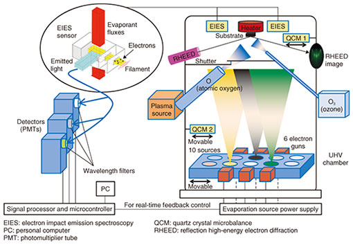
1. Significance of research on novel functional materialsThe development of novel functional materials has been contributing to advances in fundamental science as well as the development of new and/or high-performance devices; the latter has sometimes brought about breakthroughs even in the design concept of devices and has had a substantial impact on our societies. Examples of such novel materials include superconducting oxides (Nobel Physics Prize in 1987); fullerenes, a football-like structure comprising 60 carbon atoms (Nobel Chemistry Prize in 1996); graphene, an extremely thin graphite layer of single-atom thickness (Nobel Physics Prize in 2010); and nitride semiconductors, the essential constituents of blue light-emitting diodes (LEDs) (Nobel Physics Prize in 2014). In fact, some alternative materials have been proposed to overcome the limits of miniaturization in silicon (Si)-based integrated circuits (Moore’s law limit) [1]. Another good example is InP (indium phosphide), rather new compared with Si and gallium arsenide (GaAs), which is essential for ultrahigh-speed-operable optical devices in optical communications [2]. The development of novel functional materials and fabrication of devices exploiting them are always challenges, and one has to start with basic research. To achieve designated but yet-unrealized functions, two approaches are possible. One is to create/synthesize brand-new materials/compounds, and the other is to improve the quality of some already existing materials and alternately stack them followed by processing in the nanometer range. Tremendous efforts have been made here at NTT Basic Research Laboratories using both approaches. We have been exploiting our unique and state-of-the-art apparatuses and technologies for materials creation, which, at least partially, we developed through our own efforts. In the Feature Articles in this issue, we describe our latest accomplishments in such materials science research. Because of space limitations, we regrettably had to omit recent developments in bio-soft materials research previously featured in 2016 [3]. 2. Materials creation using thin-film synthesis methodsIn this section, we explain what thin-film specimens are and how they are prepared. 2.1 Thin-film specimensThe phrase synthesis of novel materials may bring to mind reactions of reagents in beakers and flasks as well as calcination and sintering of various ingredient powders in furnaces. However, our approach involves synthesis by means of thin-film growth methods. Generally, thin films are specimens whose thicknesses are in the range between 0.1 nm (atomic monolayer) and 10 µm; here, 1 nm is 1/1000 µm, and 1 µm is 1/1000 mm. Researchers and experts use the term growth for the preparation of films, as our thin-film specimens are grown on single-crystalline substrates in an atomic- or molecular-layer-by-layer manner, leading to single-crystalline thin films. Note that solids in which atoms are periodically and orderly arranged and thus form lattices are called crystals, and crystals that have only a single atomic arrangement over an entire volume are called single crystals. 2.2 Thin-film growth methodsWe have mainly adopted two kinds of thin-film growth methods: molecular beam epitaxy (MBE) and metal-organic vapor phase epitaxy (MOVPE); the term epitaxy comes from the Greek roots epi, meaning above and taxis, meaning an ordered manner. In MBE, thin films are formed on heated single-crystalline substrates in an ultrahigh vacuum (UHV) chamber (~10 trillion times lower than the atmospheric pressure) by reaction between the constituent elements that are supplied as atomic or molecular beams. In MOVPE, thin films are also formed on heated single-crystalline substrates but in a reactor furnace, in which metal-organic substances containing the constituent cations are flowed with a carrier gas, for example, H2 (hydrogen gas) or N2 (nitrogen gas), along with an anion source gas, for example, NH3 (ammonia gas). The latter method belongs to a broader category called chemical vapor deposition (CVD), where the metal-organic sources are not necessarily used. Both methods were originally developed for growing high-quality thin films of known materials and also for fabricating junctions and superlattices consisting of various known materials. To search for brand-new materials that are non-existent in nature, MBE is the more suitable method, as the film growth proceeds under conditions far from the thermodynamic equilibrium. Actually, as exemplified in the Feature Articles in this issue, MBE is used to fabricate the brand-new ferromagnetic material Sr3OsO6 (Sr: strontium, Os: osmium, O: oxygen) [4], as well as CaCuO2 (Ca: calcium, Cu: copper, O: oxygen) having the infinite-layer structure (IL-CaCuO2) [5], c-BN (cubic-structured boron nitride) [6], and lightly erbium-doped CeO2 (cerium oxide) thin films [7]; IL-CaCuO2 and c-BN are thermodynamically metastable, and high pressure is required to synthesize them in bulk forms. In contrast, in MOVPE and CVD, thin-film growth proceeds under conditions close to the thermodynamic equilibrium, and, hence, dislocation density in the thin films can be reduced. This means that high-crystalline-quality films are rather readily achieved. Accordingly, MOVPE has been widely exploited in the fabrication of nitride-based light-emitting devices and transistors, for example, GaN (gallium nitride)-based devices. Two of the Feature Articles in this issue explain the fabrication of atomic-layer-thick graphene and h-BN (hexagonal boron nitride) by CVD [8] and GaP (gallium phosphide) nanowires by MOVPE [9]. 3. MBE as a synthesis method sui generis for brand-new materialsNTT Basic Research Laboratories is one of the most advanced research organizations in the world, in that some brand-new materials have been synthesized using MBE. MBE is a thin-film growth technique developed in the late 1960s to crystallize and investigate GaAs epilayers and has been applied to grow thin epitaxial structures made of various known materials. Here, we start with an explanation of how the unique characteristics of our MBE apparatuses allow for the creation of novel materials. A schematic illustration of our MBE set-up sui generis, which is totally tuned up for the growth of multi-cation oxides (complex oxides) [10], is shown in Fig. 1.
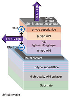
One of the unique features of our MBE system is that the flux rates of multiple cations supplied at a certain moment are simultaneously monitored and the results are fed back in real time to the power supplies of the evaporators, which allows for precise control and stable supply of the atomic fluxes of each constituent cation; the flux rates are monitored by electron impact emission spectroscopy (EIES). In EIES, atomic fluxes are impacted with accelerated electrons, and each flux emits light of characteristic wavelengths. Although the intensity of the emitted light is too weak to detect with the human eye, the EIES equipment can measure the intensity of the emitted light in a wavelength-specific manner and transform the optical signals into electrical ones. In this manner, one can obtain information on what and how many atoms are supplied. It is worth mentioning that the principle of EIES takes after that of a flame reaction, which may have been learned in one’s high school days. Instead of being impacted with electrons, a flame reaction takes place when materials are heated in a flame. In doing so, light with element-specific wavelengths is emitted, for example, greenish yellow light for Ba (barium) and bright red light for Sr (strontium). The flame reaction is utilized in fireworks, where one can enjoy multiple combinations of beautiful colors achieved by various combinations of pyrotechnic materials. Another characteristic feature of our MBE system is the capability of introducing reactive atomic oxygen (O) or ozone (O3) gas, which enables oxidation of the cation species under UHV; typically, oxygen exists as O2 (oxygen molecules). We can also grow nitride thin films, for example, c-BN, if the oxygen gas source is replaced by an atomic nitrogen (N) gas source [11]. Furthermore, modern MBE systems are equipped with a reflection high-energy electron diffraction (RHEED) capability, which is also the case with ours and allows for real-time monitoring of crystal structure and crystallinity of thin films during the growth. In RHEED, a high-energy electron beam is incident to the sample surface under grazing incident angle, and hence, this method is surface sensitive. As the operation of RHEED requires a high vacuum, RHEED is a method highly compatible with MBE. Note that in our labs, we can also monitor thin-film growth in real time with MOVPE using a method other than RHEED. These advantages of our MBE system have enabled us to discover novel superconductors [12, 13] and a magnetic material [14], while some important growth parameters such as the flux ratio of cations, substrate materials, substrate temperature, and oxidation strength are systematically varied. Outstanding developments in measurement techniques and equipment are another important factor that has enabled materials science research using thin-film specimens. Nowadays, cutting-edge characterization methods can be applied to thin-film specimens due to their sufficiently high sensitivity. Since the thicknesses of thin-film specimens are limited to, at most, a few hundred atomic/molecular layers, detailed investigation of their properties had been elusive until a couple of decades ago even when one succeeded in synthesizing new materials in thin-film forms. In stark contrast, atomic-resolution scanning transmission electron microscopes as well as magnetometers with an ultrahigh sensitivity adequate for investigating the magnetic properties of 300-nm-thick specimens have been developed and exploited in our daily research, as represented by the accomplishments presented in these Feature Articles. The use of thin-film specimens in the search for novel materials has the following advantages as compared with bulk specimens: less consumption of reagents (less use of natural resources), higher-throughput screening, and higher compatibility with device fabrication processes. 4. Functionalization: from material synthesis to device fabricationTo achieve devices that exhibit designated functions by exploiting various properties inherent to individual materials, just the existence of certain materials or the availability of their thin films is not enough. We explain here the functionalization and device fabrication processes using an aluminium nitride (AlN)-based LED as an example of a typical semiconductor device (Fig. 2). The AlN-based diodes emit light with the shortest wavelength among any solid-state semiconductor-based light sources, as has been described in a previous NTT Technical Review article [15].
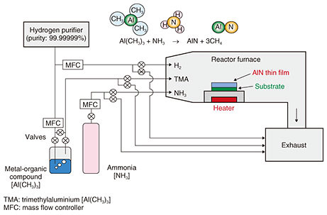
The AlN-based LEDs are prepared by MOVPE (Fig. 3). The existence of the chemical substance, AlN, had been well-known, and accordingly, AlN itself is not a new material. However, to make AlN usable as a functional semiconducting material requires the accumulation of a vast amount of research, which is comparable to that for the creation of new materials.
First, the crystalline quality of AlN itself needs to be substantially improved (Phase I). This is because the emergence of inherent functionality is hindered when (thin-film) crystals include polycrystalline portions and/or a high density of defects. Next, doping control is required (Phase II). To fabricate LEDs, or more generally, some semiconductor-based devices, it is necessary to deliberately introduce heterovalent impurities into pristine materials (here, AlN) and achieve a situation in which positive and negative carriers (holes and electrons, respectively) exist in different regions. Accordingly, in phase II, research efforts are focused on how to achieve effective doping without dramatically deteriorating the crystallinity of the thin films. Finally, the design and fabrication of stacking structures (schematically shown in Fig. 2) need to be investigated (Phase III). For example, one should optimize the thickness of each stacking layer and the number of repetition periods in the superlattice layers. In addition, the stacking layers are lithographed and and etched until device structures exhibiting certain functions are eventually completed. 5. Towards further creation of novel functional materialsAs described above, materials science research requires vast amounts of time and effort as well as long-term strategies [16]; it follows the saying, “Endurance makes you strong.” This is especially true for research on the creation of hitherto-undiscovered materials but with fascinating properties. Such research may be likened to Phase Zero, and is sometimes compared to a journey for seeking the Holy Grail, borrowing the phrase of Prof. Emeritus M. R. Beasley of Stanford University. Nevertheless, materials science research is a dreamful activity that inherently has the potential for yielding something exciting, as far as taking methodologically correct approaches. For example, on the assumption that a useful room-temperature superconductor is discovered, it will lead to disruptive innovation [17] that allows for lossless direct current power feeding as well as lossless intra- and inter-chip connections. Materials science research has relied on the three conventional paradigms of science: experiment, theory, and computation. Individual materials are first synthesized and characterized. Their molecular/crystal/electronic structures are subsequently determined with the aid of theoretical and computational studies. Finally, functional structures and/or devices are designed and fabricated. Recently, a fourth paradigm called materials informatics (MI) has emerged, where the compositions and structures of materials having desired functions are predicted by utilizing machine learning techniques along with materials databases and/or theoretical calculations [18]. While further progress in MI is desirable to see its bona fide capability and potential, we hope to promote our materials science research further by combining our advantages of thin-film synthesis technologies already in hand and the newly developed approach, MI. References
|
||||||||||||||||||||||||||||||||||||||