|
|||||||||||||||
|
|
|||||||||||||||
       |
Special Feature: KTN Crystal Technologies Vol. 7, No. 12, pp. 16–20, Dec. 2009. https://doi.org/10.53829/ntr200912sf3 KTN Crystals Open Up New Possibilities and ApplicationsAbstractBy exploiting the giant electro-optic effect of potassium tantalate niobate (KTN) crystal, we have developed a wide-angle fast optical beam scanner and a fast varifocal lens. These devices are applicable not only to optical communications, but also to various other fields that use optical beams, so we are seeking sales scenarios for KTN devices. 
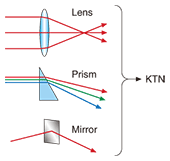
1. IntroductionLight is identified by its wavelength, intensity, polarization, phase, and propagation direction. Therefore, any devices that use light manipulate some of these characteristics. For example, lenses, prisms, and mirrors change the propagation direction of light, displays change its intensity, and holography manipulates its phase. Potassium tantalate niobate (KTN) crystals can manipulate all of these characteristics. In particular, we would like to emphasize the quick response of their propagation-direction-changing capabilities. It means that KTN could take the place of fundamental optical devices such as lenses, prisms, and mirrors (Fig. 1), when they need to operate at high frequencies.
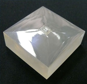
2. Basic properties of KTNKTN is an oxide of potassium (K), tantalum (Ta), and niobium (Nb). Its chemical formula is KTa1-xNbxO3. It has been known since the 1950s that KTN has a very large electro-optic effect; that is, its refractive index is changed greatly by a comparatively low applied voltage. To be used as an optical device, the KTN must be a single crystal so that the incident light does not scatter. However, growing single crystals of KTN has been extremely difficult, which has prevented KTN from entering practical use. NTT Photonics Laboratories has developed a KTN crystal growth technique and in 2003 it was mature enough to consistently give high-quality large KTN single crystals (Fig. 2) [1].
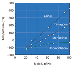
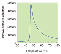
KTN has four different crystallographic structures depending on the temperature: rhombohedral, monoclinic, tetragonal, and cubic from low to high temperatures, as shown in Fig. 3. KTN optical devices are used at temperatures a few degrees above the tetragonal-to-cubic transition temperature. By changing the Ta:Nb ratio in KTN, we can control its transition temperature and set the operating temperature to room temperature by choosing x = 0.35. An example of the temperature dependence of the relative dielectric constant is shown in Fig. 4, where the relative dielectric constant reaches 50,000 at the transition temperature of 47°C.
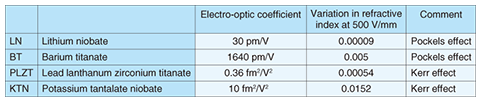
The variation in refractive index δn caused by an applied electric field is given by  This tells us that δn is proportional to the square of the applied electric field E , where n0 is the refractive index, ε0 is the dielectric constant in vacuum, and εr is the relative dielectric constant. The fact that the temperature dependence of εr in Fig. 4 has a sharp peak means that KTN can be used for applications where the use of temperature controllers can be afforded. Since it is important to reduce the cost of temperature control, we chose a Nb content that sets the operating temperature to a few degrees above room temperature, which allows us to use a microheater instead of a Peltier cooler. The reason the KTN in Fig. 2 looks opaque is that the picture was taken at room temperature, so the KTN was tetragonal. In the tetragonal structure, a lot of ferroelectric domains scatter light. On the other hand, KTN becomes transparent when the temperature is raised and it transforms into the cubic structure. The electro-optic effects in typical materials are compared in Table 1. Lithium niobate (LN) and barium titanate (BT) show the Pockels effect, which means that the variation in the refractive index is proportional to the electric field. LN is used in optical communications and BT is used in laboratories for optics studies. Lead lanthanum zirconium titanate (PLZT) and KTN show the Kerr effect, which means that the variation in refractive index is proportional to the square of the applied electric field. Although the Pockels effect exceeds the Kerr effect when the applied field is low, the Kerr effect is stronger at higher fields. The comparisons in Table 1 are for a practical electric field value of 500 V/mm. They show that the electro-optic effect of KTN is outstanding. This means the KTN lets you reduce the voltage or the device size when you do something using its electro-optic effect.
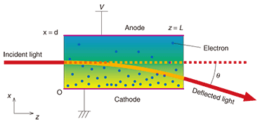
3. Fast optical beam scannerNTT has discovered a special electro-optic effect, called the space-charge-controlled EO effect, in KTN [2]. When the electrodes are made of titanium, electrons are injected into the KTN from the cathode (Fig. 5) to form an electric field with a gradient given by  where x is the distance from the cathode, V is the applied voltage, and d is the thickness of the KTN. Using Eq. (1), we obtain the variation in refractive index as  It is proportional to x, which implies that the KTN changes the optical beam’s propagation direction without deforming its shape, just like prisms do. Since this phenomenon arises from an electrical process, it is very fast compared with mechanical devices such as galvano-mirrors, polygon mirrors, and microelectromechanical systems (MEMS) mirrors. Thus, KTN can provide the basis for a fast optical beam scanner.
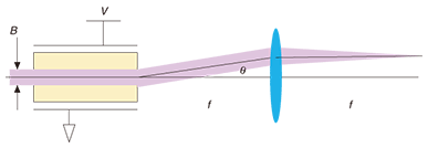
The space-charge-controlled EO effect in KTN causes the beam deflection angle θ to accumulate as the light travels in the crystal:  where L is the light propagation length in KTN. For a typical case such as d = 1 mm, L = 6 mm, and εr = 30,000, the deflection angle reaches ±128 mrad (±7.3°) at V = ±400 V. This voltage is fairly small compared with that of the conventional EO deflector, which needs tens of thousands of volts. We have confirmed the response time of less than 1 μs for a single pulse and for 100-kHz continuous operation. As shown in Fig. 4 and Eq. (1), since the large electro-optic effect arises from the large dielectric constant, we should regard the KTN as working as a capacitor when we operate it at high frequency. For example, a typical KTN crystal with a size of 5 mm × 6 mm × 1 mm has a capacitance as large as 8 nF, which requires a current of 2 A for 100-kHz, 400-V operation. It is not difficult to make a resonant circuit for constant frequency operation in order to make a short pulse generator for low-frequency triggering. However, it is necessary to develop a high-performance amplifier for fast, high-frequency random operations. We must also consider the resolution of the scanner. The deflection angle is proportional to V2/d3, as given by Eq. (4), which means that the applied voltage increases as the 1.5th power of the KTN thickness to maintain the same deflection angle. Therefore, thinner KTN allows a much lower applied voltage. However, the resolution deteriorates as the KTN thickness is reduced, as shown in Fig. 6. If we let the beam diameter be B and the maximum deflection angle be θ and we place a lens of focal length f at a distance f from the KTN, then the beam is focused at a distance 2f from the KTN. The diameter of the focused spot is given by 2.4fλ/B. Since the scanning range at the focal plane is 2ftanθ, the resolution is defined by 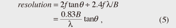 The resolution is independent of the focal length. For example, the theoretical resolution is 41 when the wavelength is 532 nm, the beam diameter is 0.25 mm, and the scanning angle is ±5°. A detailed analysis considering KTN properties is given in “High-resolution KTN Optical Beam Scanner” in this Special Feature [4].
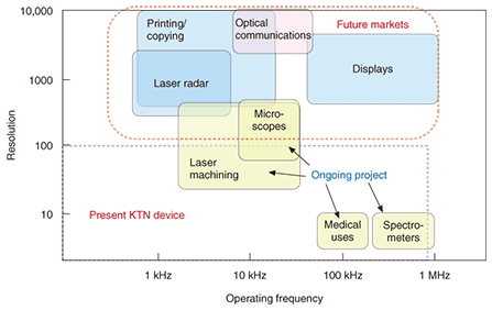
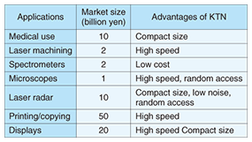
Moreover, various factors such that the transition temperature are not homogeneous, so the deflected beam is reflected at the electrode surface when the KTN is thin and the saturated polarization deforms the beam when KTN is thick, making it difficult to enhance the resolution by the simple method depicted in Fig. 6. Therefore, we are examining various methods of increasing the resolution. One of them is introduced in “High-speed Spectrometer Using KTN Optical Beam Scanner” in this Special Feature [5]. 4. Fast varifocal lensWhen the electrodes are made of gold or platinum, electron injection is suppressed, so the usual electro-optic effect appears. By devising a special electrode structure, we have successfully made a KTN varifocal lens with a focal length that changes with the applied electric field. While the response time of the conventional varifocal lens is slower than 1 ms, our KTN varifocal lens has been experimentally measured to respond faster than 1 μs. A detailed discussion is given in “Fast Varifocal Lenses Based on KTa1-xNbxO3 (KTN) Single Crystals” in this Special Feature [6]. By using both the KTN varifocal lens and the KTN optical beam scanner in combination, we can now address an optical spot in three-dimensional space within 1 μs. 5. Various applications of KTN devicesSince KTN devices manipulate the propagation direction of light, they can be applied not only to optical communications, but also various fields that use optical beams. Applications are mapped against resolution and operating frequency in Fig. 7 and the advantages of KTN for each application are listed in Table 2. The resolution of the present KTN devices is insufficient for printers, copiers, and displays, which are large markets. Therefore, we need to continue to enhance the resolution. On the other hand, the present resolution is sufficient for spectrometers and medical use, and it matches the achievable range for laser machining and microscopes. For these possible applications, we are now examining other properties such as long-term reliability, beam quality, usable wavelengths, and high power durability. Although long-term reliability is crucial for optical communications and laser radars because it is difficult or troublesome to repair such equipment, we are first focusing on medical uses because these involve saving human lives. We are currently at the first stage of analyzing the deterioration mechanism. To meet the various demands for KTN optical beam scanners, we are going to increase their resolution and examine the individual specifications needed for each application.
References
|
||||||||||||||