|
|||||||||||||||||||||||
|
|
|||||||||||||||||||||||
       |
Feature Articles: Circuit and Device Technologies for Extremely Low-power Consumption for Future Communications Systems Vol. 11, No. 2, pp. 5–10, Feb. 2013. https://doi.org/10.53829/ntr201302fa1 Device Innovations toward the Green of Information and Communications TechnologyAbstractThe recent growth in popularity of fiber-to-the-home (FTTH) services and mobile smartphones is resulting in an explosive increase in the volume of communications traffic, and this has led to a subsequent increase in the power consumed by network devices and terminals. In the Feature Articles in this issue, we give an overview of power-reducing and power-saving techniques to implement green information and communications technology, and we introduce technological developments NTT is working on that are designed to reduce the power consumption of network equipment.
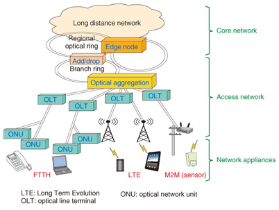
1. IntroductionIn Japan, the simultaneous proliferation of optical fiber-to–the-home (FTTH) services such as B FLET’s and high-speed mobile communications services such as Xi (pronounced crossy) has led to widespread daily use of the “anywhere, anytime” Internet access. Many users are now reaping the benefits of leading-edge broadband networks, anticipating the expansion of new application services and innovative terminal devices, and looking forward to further improvements in information and communications technology (ICT) that give them a higher quality of life (QoL). Against this background, the volume of communications traffic centered on image- and video-related services is growing explosively, and it is therefore important to find ways of ensuring that the power consumed by related equipment does not increase. We believe that power reduction is an important research and development challenge in the drive for continuous development of network services that support the creation of an affluent society. 2. Ongoing research and development in Microsystem Integration LaboratoriesIn November, 2010, the NTT Group drew up a new environmental vision called THE GREEN VISION 2020 [1] for intended application through 2020. We are continuing with our initiatives and research and development (R&D) with the aim of forming a recycling-oriented society by implementing Green of ICT and applying Green by ICT [1]. In our R&D on circuits and devices for communications at NTT Microsystem Integration Laboratories, we are developing technology that not only prevents any increases in power consumption but also reduces power consumption while simultaneously improving device functionality and performance. We are also conducting innovative research with the aim of achieving extreme power saving systems. An optical IP (Internet protocol) network is divided into three segments: a core network that covers a wide area, access networks that extend from the core, and network appliances that are connected to the access networks (Fig. 1). Of these segments, the access networks consume the largest proportion of power [2], and methods to save power in the access networks are being investigated. R&D is underway on media access control (MAC) large-scale integrated circuits (LSIs) for the 10-Gbit/s Ethernet passive optical network (10G-EPON) systems that will be the next upgrade of the FTTH service. Our objective in this research is to achieve reduced power consumption through innovations in circuit architecture and reductions in circuit scale. We are also implementing sleep control functions for optical network units (ONUs) that are expected to have a substantial effect on power saving, and are conducting experiments in order to evaluate the effectiveness of these techniques. On the user side, a trend toward a reduction in the normal usage frequency (operating time) of devices has been observed, so there is much leeway in saving electrical power when devices are not in use.
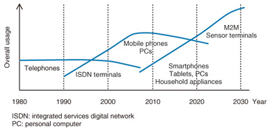
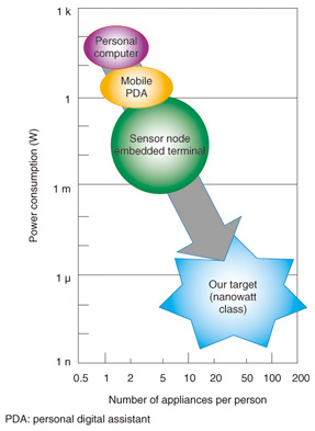
In core networks, traffic from the access networks is aggregated, and devices such as core routers are required to efficiently accommodate functions for processing large volumes of data in compact equipment. In this case, efforts to reduce power benefit the environment and energy resources and also alleviate design margins relating to heat generation of communications installations. This technology is expected to help reduce installation space requirements, capital expenditure (CAPEX), and operating expenses (OPEX) by enabling high-density installation. With network appliances, the focus is on reducing power in mobile and sensor terminals. Power-saving technology is directly related to the extension of battery life and will help to improve user-friendliness and reduce maintenance work. The transition in the types of network appliances used over the years is shown in Fig. 2. We predict that a huge variety of sensor terminals in the machine-to-machine (M2M) communications form will be widely distributed in the future. Consequently, we are carrying out R&D on ways to achieve much higher levels of power saving in terminal architecture and configuration technology, as well as R&D on energy harvesting technology.
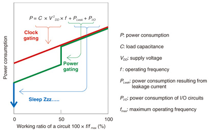
3. LSI power-reduction technology and directions of R&DHere, we review techniques to reduce power consumption through the appropriate design of large-scale integrated circuits (LSIs), which form the heart of signal processing and communications protocol control equipment. In terms of device technology, we could use compound semiconductor technology or SiGe bipolar complementary metal oxide semiconductor (Bi-CMOS) technology for communication LSIs in the transmitters and receivers of transceivers to improve speed. If we were to focus on power instead, we could use silicon CMOS technology to implement large-scale circuits that provide advanced digital signal processing or communications protocol control. We review the power consumed by CMOS circuitry below. The power consumed by a CMOS digital circuit can generally be written as: P = C VDD2 f + PLeak + PI/O The first term on the right side represents the electrical power consumed through repeated charging and discharging that occurs with the operation of the logic circuitry. The second term is the power dissipation due to leakage current, which has increased as transistors have become smaller and which will dissipate power through leakage despite our best efforts to prevent it. The third term is a characteristic feature of large-capacity signal processing LSIs, which have explicitly added the power consumption of the peripheral input/output (I/O) circuit parts for moving large volumes of data into and out of LSI chips. These parts are formed by various circuits such as those that perform the serial-parallel conversion and timing control of I/O signals and the analog circuits that drive external loads. The power consumption reaches particularly high values in LSIs that input and output large quantities of frames or packets when processing large volumes of signals. This is a continuing major issue in implementing larger throughputs and higher integration levels. In the first term of the equation, C is the load capacitance of the logic gates (basic circuitry). This also depends on the layout of the wiring, but as a rule of thumb, the value is determined once the generation (nodes) of the fabrication process has been determined. The value VDD is the power voltage, which has dropped from 5 V to 3.3 V as processes have become finer, leading to a corresponding decrease in power consumption. When the latest processes are used, the internal digital circuits are designed to run with a power voltage on the order of 1 V. In addition, f is the actual operating speed (frequency) of the circuitry. If we focus on f, it is clear that the first term can be reduced by lowering f, if it is acceptable for circuit operations to become sluggish or even stop temporarily, depending on the communications situation. This situation is shown schematically by the red line in Fig. 3. Control of f can be achieved by clock gating that stops the clock that is distributed to the circuitry, either temporarily or partially.
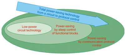
The power dissipation caused by leakage current (second term of equation) cannot be reduced by clock gating but must be reduced by cutting the power supply. Shutting off power either temporarily or partially is known as power gating. Circuit technology that uses power gating is referred to as multithreshold voltage CMOS (MTCMOS) technology and is well known as an NTT innovation [4]. Skillful use of power gating makes it possible to supply power to necessary functions only when needed, and to let the device sleep when it is not required. This is shown schematically by the green and blue lines in Fig. 3. It may also be possible to implement even finer-tuned power saving by re-examining communications control or by exerting control over the state of traffic that should be processed. The power-saving technique linked to this communications control (Fig. 4) is one of the technological development trends in power reduction based on circuit technology for communication LSIs.
4. Topics and structure of feature articlesThe other Feature Articles in this issue introduce six topics we are working on at NTT Microsystem Integration Laboratories. The second article, “Low-power LSI Techniques for Next-generation FTTH System” gives a detailed description of power reduction technology for control LSIs for the 10G-EPON system [5]. It introduces our efforts to reduce power by scaling down signal processing and communications control circuits. It also introduces the possibility of power-saving in the analog circuits that drive lasers according to the data traffic situation, by burst signal processing technology, which is our technological strength. The third article, “Energy-saving Technique for High-speed Packet Forwarding LSI” describes a power gating technique for achieving both high throughput and energy-saving performance of a 100-Gbit/s-class high-end router packet-forwarding circuit [6]. The technique uses two parallel forwarding engines that are fully activated when the traffic is heavy and partially powered down depending on the traffic conditions. The next three articles deal with topics relating to M2M sensor terminals. “Nanowatt Circuit Technology for an Ultrasmall Wireless Sensor Node with Energy Harvester” introduces details of investigations targeted at extremely low-powered sensor terminals [7]. The goal is to develop sensor terminals that are able to gather electrical power from the surrounding environmental energy, enabling them to operate autonomously and perpetually. This article also proposes sensing circuits and wireless transmission circuits operating on the order of nanowatts. (Fig. 5)
The article entitled “Low Power Consumption Sensor Interface Terminal for Various Telemetry Applications” describes terminal configuration technology that can be applied to existing services and that can accommodate a variety of sensors [8]. Devices for telemetry must be able to operate under battery power for five to ten years without maintenance. It is therefore a technological challenge to determine how they will best be able to respond to such conditions. The article “Vibrational Energy Harvesting with Microelectromechanical System Technology” introduces attempts to harvest electrical power from vibration energy that is all around us and provides details relating to research into circuits that operate on electrical power on the order of nanowatts [9]. We report on details and the current situation of vibration power-generating technology used in microelectromechanical systems (MEMS) technology. Finally, in “Integrated Silicon-based Optical Interconnect for Fast, Compact, Energy-efficient Electronic Circuit Systems” [10], we introduce the state of R&D into silicon photonics technology that will be used to convert the input-output interfaces of devices that handle large volumes of signals to fiber optics, reduce the previously described power consumption term PI/O, and also attempt to help make devices even more compact and highly integrated by integrating and combining optical and electrical processing. References
|
||||||||||||||||||||||